Strain-Stable Electronics: Achieving Reliable Electrical Performance in Wearable and Implantable Biomedical Devices
This comprehensive article addresses the critical challenge of maintaining stable electrical performance under mechanical strain for biomedical applications.
Strain-Stable Electronics: Achieving Reliable Electrical Performance in Wearable and Implantable Biomedical Devices
Abstract
This comprehensive article addresses the critical challenge of maintaining stable electrical performance under mechanical strain for biomedical applications. It explores the foundational principles of strain effects on materials, details methodological approaches for design and fabrication, provides troubleshooting strategies for common failure modes, and offers validation frameworks for comparing emerging technologies. Aimed at researchers, scientists, and drug development professionals, the content synthesizes recent advances to guide the development of robust wearable sensors, bio-integrated electronics, and implantable devices for continuous health monitoring and therapeutic intervention.
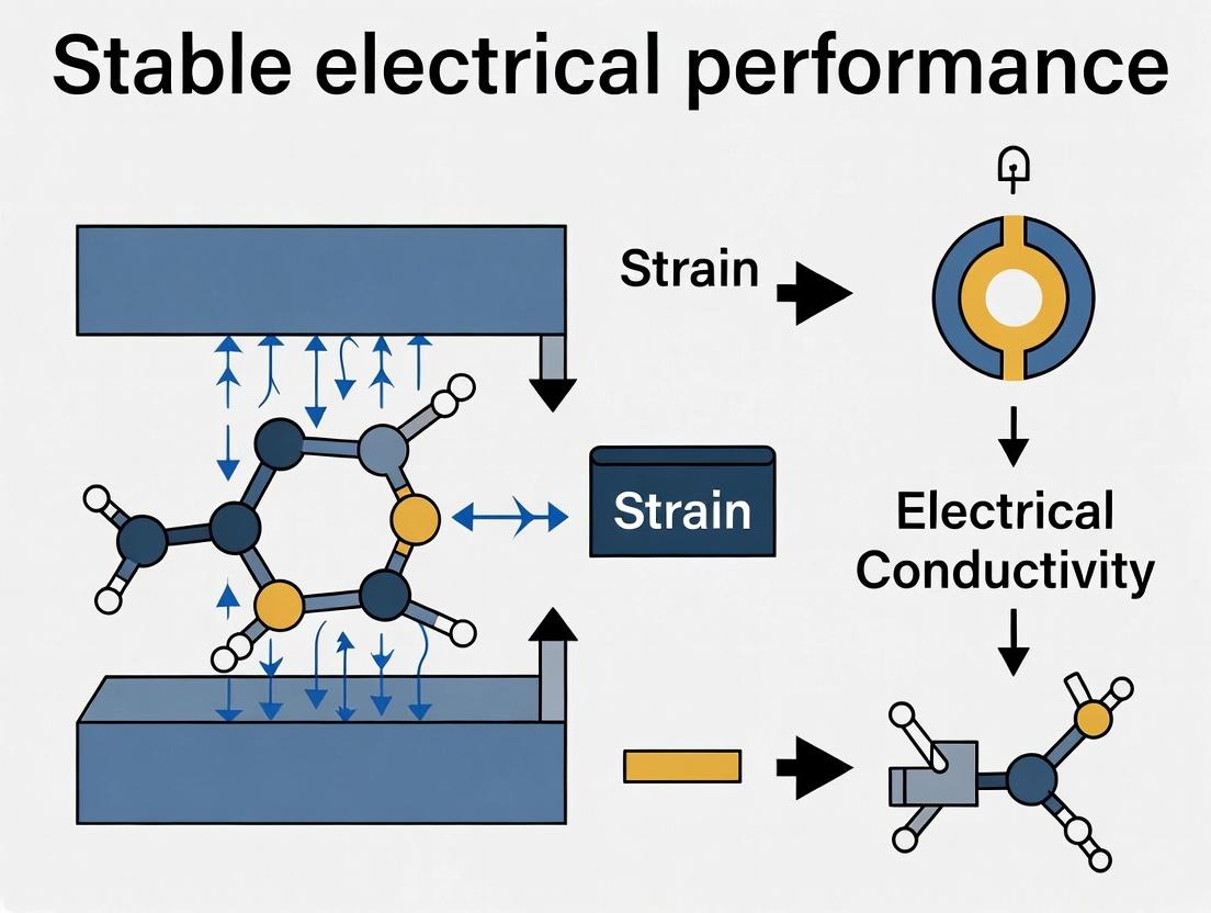
Understanding the Strain-Performance Conundrum: Mechanisms and Material Science Foundations
Technical Support Center: Troubleshooting & FAQs
This support center is designed to assist researchers working within the broader thesis context of achieving stable electrical performance in flexible/stretchable electronics and bioelectronic interfaces under dynamic mechanical strain. The guidance addresses common experimental challenges in characterizing key metrics such as resistance change (ΔR/R₀), gauge factor (GF), hysteresis, and drift.
Troubleshooting Guides
Issue 1: Excessive Noise in Resistance Measurements Under Cyclic Strain
- Symptoms: Erratic fluctuations in recorded resistance/current, obscuring true signal from strain application.
- Potential Causes & Solutions:
- Poor Contact Integrity: Unstable wire bonding or clipped contacts create intermittent connections.
- Protocol: Re-establish all electrical contacts. For thin-film devices, use silver epoxy or re-solder connections. For wearable setups, ensure consistent skin-electrode impedance with fresh electrolyte gel.
- Electromechanical Artifacts: Movement of measurement cables themselves induces triboelectric or electromagnetic noise.
- Protocol: Secure all cables along the strain direction using non-conductive tape to minimize independent movement. Use shielded cables and ground the shield properly.
- Insufficient Signal Filtering: Electrical noise from equipment or environment is overwhelming the low-amplitude signal.
- Protocol: Implement a low-pass filter in your data acquisition (DAQ) system. Set the cutoff frequency just above the maximum frequency of your applied strain waveform (e.g., for a 1Hz strain cycle, a 10Hz cutoff is appropriate).
- Poor Contact Integrity: Unstable wire bonding or clipped contacts create intermittent connections.
Issue 2: Inconsistent Gauge Factor Calculation Across Samples
- Symptoms: High variability in calculated GF (GF = (ΔR/R₀) / ε) for identical materials or devices.
- Potential Causes & Solutions:
- Inaccurate Strain (ε) Measurement: Assuming applied actuator displacement equals sample strain.
- Protocol: Use a non-contact method (e.g., digital image correlation with speckle pattern, laser extensometer) to measure actual local strain on the active material region. Do not rely on actuator displacement alone.
- Non-Ohmic Contact Effects: The measured resistance includes contact resistance, which may not scale linearly with strain.
- Protocol: Perform 4-point probe (Kelvin) measurements to isolate the intrinsic resistance of the active material from the contact resistance.
- Material Inhomogeneity: Variations in film thickness, nanoparticle dispersion, or polymer crystallinity.
- Protocol: Characterize material uniformity prior to electrical testing (e.g., SEM for morphology, profilometry for thickness mapping). Report GF as a mean value with standard deviation across multiple (n≥5) devices.
- Inaccurate Strain (ε) Measurement: Assuming applied actuator displacement equals sample strain.
FAQs
Q1: How do I differentiate between reversible hysteresis and permanent drift in my electrical signal under repeated stretching? A: This is a core metric for stability. Conduct a controlled experiment:
- Protocol: Apply 100-1000 cycles of a constant-amplitude, constant-frequency tensile strain (e.g., 10% strain at 0.5Hz). Record resistance continuously.
- Analysis: Plot Resistance vs. Time and Resistance vs. Strain (loop plot).
- Hysteresis: Manifests as a repeatable separation between the loading and unloading curves in the loop plot. Its width can be quantified.
- Drift: Observed as a progressive, non-recoverable shift in the baseline resistance (R₀) or the mean resistance value over time on the time-series plot. Calculate drift rate as % change per cycle.
Q2: What is the standard way to report "stability" for a strain-sensing material in a comparative table? A: Stability should be reported using multiple, clearly defined quantitative metrics from a standardized test. A summary table is essential.
Table 1: Key Quantitative Metrics for Reporting Electrical Performance Stability Under Dynamic Strain
| Metric | Definition | Typical Idealized Target | Measurement Protocol Summary |
|---|---|---|---|
| Gauge Factor (GF) | Sensitivity: (ΔR/R₀) / ε | High & consistent across strain range | Measure ΔR/R₀ at known, measured ε (via 4-point probe & DIC). |
| Hysteresis (%) | (ΔRhyst / ΔRmax) * 100 at a given ε | < 5% | Calculate from width of stable R-ε loop after conditioning cycles. |
| Drift Rate | % change in baseline R₀ per cycle or per time | < 0.1%/cycle | Monitor R₀ over N cycles (e.g., 1000), fit linear trend. |
| Cycle Lifetime | Number of cycles before critical failure (e.g., ΔR/R₀ > 50% shift) | > 10,000 cycles | Run continuous strain cycles until failure criterion is met. |
| Response Time | Time to reach 90% of final ΔR upon strain application | < 100 ms | Apply a step strain, record high-speed resistance data. |
Q3: My conductive polymer composite's resistance doesn't return to baseline after strain release. Is this creep, plastic deformation, or material damage? A: Follow this diagnostic protocol:
- Visual Inspection: Use optical microscopy to check for cracks, delamination, or permanent necking.
- Mechanical Test: Perform a pure mechanical stress-strain cycle on a separate sample. If permanent deformation is seen, the matrix has yielded.
- Electrical-Mechanical Test: Perform a low-strain cycle (e.g., 1%). If resistance returns to baseline, but does not at higher strains, the cause is likely microcrack formation or permanent disruption of the conductive network. If resistance slowly creeps back over minutes/hours, it is likely viscoelastic polymer recovery affecting the conductive pathways.
The Scientist's Toolkit: Research Reagent & Materials
Table 2: Essential Research Reagents & Materials for Dynamic Strain-Electrical Performance Experiments
| Item | Function & Rationale |
|---|---|
| Polydimethylsiloxane (PDMS) | Ubiquitous elastomeric substrate. Allows control of modulus, surface chemistry, and optical transparency for in-situ observation. |
| Ecoflex Gel | Ultra-soft silicone elastomer. Used for simulating bio-tissue interfaces or achieving very high (>100%) strain regimes. |
| Silver/Silver Chloride (Ag/AgCl) Paste | Stable reference electrode material and conductive paste for biological or ionic liquid-based strain sensing systems. |
| Carbon Nanotubes (CNTs) / Graphene Flakes | Conductive nanofillers for composites. Provide piezoresistive behavior; dispersion quality is critical for performance. |
| Poly(3,4-ethylenedioxythiophene):Poly(styrene sulfonate) (PEDOT:PSS) | Conductive polymer. Used for intrinsically stretchable conductive films; performance modulated by secondary dopants. |
| Digital Image Correlation (DIC) System | Non-contact optical method to map actual strain field on deforming sample, critical for accurate GF calculation. |
| Programmable Linear Actuator | Applies precise, reproducible, and cyclic uniaxial strain to the test sample. |
| Source Meter Unit (SMU) / 4-Point Probe Station | Provides accurate, low-noise sourcing and measurement of voltage/current, essential for stable resistance tracking. |
Experimental Workflow & Pathway Visualization
Title: Workflow for Characterizing Electrical Stability Under Strain
Title: Signal Pathways from Mechanical Strain to Electrical Output
Troubleshooting Guides & FAQs
Q1: During a tensile strain experiment on a metallic thin film, my measured resistance decreases initially but then increases unpredictably. What could be the cause?
A: This is a common issue in strain-dependent electrical measurements. The initial decrease is likely due to the alignment of micro-cracks or grain boundaries, improving contact. The subsequent unpredictable increase typically signals the onset of macro-scale cracking or defect nucleation beyond the elastic limit. To troubleshoot:
- Verify Strain Uniformity: Use digital image correlation (DIC) or a high-resolution strain gauge to confirm the applied strain is uniform across the measured section. Non-uniform bending can create localized high-strain zones.
- Inspect for Plastic Deformation: Perform a cyclic loading test (e.g., 0% → 0.5% → 0% strain). If resistance does not return to its original value, the material has undergone plastic deformation, altering its intrinsic conductivity.
- Check Contact Integrity: Ensure your four-point probe contacts are stable. Use silver epoxy or soldered contacts, and verify contact resistance remains constant throughout the experiment.
Q2: My piezocapacitive polymer sensor shows significant hysteresis—the capacitance under load differs from the capacitance when unloading. How can I minimize this for stable performance?
A: Hysteresis in capacitive strain sensors often stems from viscoelastic relaxation of the polymer dielectric and time-dependent dielectric polarization.
- Protocol for Characterization: Conduct a dynamic mechanical analysis (DMA) coupled with simultaneous capacitance measurement. This will correlate mechanical loss tangents with capacitive hysteresis.
- Mitigation Strategy:
- Material Selection: Use elastomers with lower viscoelastic loss (e.g., polydimethylsiloxane, PDMS) over highly viscous polymers (e.g., polyurethanes).
- Nanocomposite Approach: Incorporate low-concentration, high-aspect-ratio fillers like cellulose nanocrystals to reduce polymer chain mobility and provide a more elastic response.
- Measurement Protocol: Introduce a 30-60 second holding period at each strain step before recording capacitance, allowing for stress relaxation.
Q3: When applying cyclic bending strain to a flexible conductor, the electrical noise increases dramatically. How can I obtain a clean signal?
A: Increased noise under dynamic strain is frequently caused by contact fluctuation and triboelectric effects.
- Secure Interconnects: Replace clipped or pressure-based contacts with permanently bonded, flexible interconnects (e.g., anisotropic conductive film).
- Shield from Triboelectric Noise: The motion of the cable itself can generate spurious charges. Use shielded coaxial cables and secure them along the same axis as the sample bending to minimize relative movement.
- Electrical Filtering: Implement a low-pass hardware filter (e.g., RC filter with a cutoff frequency just above your signal frequency) at the data acquisition input to suppress high-frequency noise.
Q4: I observe that the gauge factor (GF) of my semiconductor strain sensor drifts over multiple measurement cycles. What is the likely mechanism and solution?
A: Drifting GF in semiconductors under strain is strongly linked to charge trapping/detrapping at defect sites and Joule heating.
- Diagnostic Experiment: Measure current-voltage (I-V) characteristics at fixed strain levels at the beginning and end of a cycling test. A change in I-V curve nonlinearity indicates trap state modification.
- Stabilization Protocol:
- Passivation Layer: Apply a thin, conformal dielectric passivation layer (e.g., atomic layer deposited Al₂O₃) to isolate the semiconductor from ambient humidity and oxygen, which exacerbate trap states.
- Current Limitation: Operate the sensor at the lowest possible sensing current to minimize Joule heating and associated defect migration.
- Pre-Cycling "Aging": Subject the device to 1000-5000 cycles of moderate strain before calibration. This can anneal some metastable defects and stabilize performance.
Table 1: Typical Gauge Factor Ranges for Different Material Classes Under Uniaxial Strain (<1%)
| Material Class | Example Materials | Typical Gauge Factor (GF)* | Key Strain Mechanism | Hysteresis (Typical) |
|---|---|---|---|---|
| Metals | Constantan, Nichrome | 2 - 5 | Geometric deformation (change in L, A) | Very Low (<0.5%) |
| Semiconductors | Silicon, Graphene, ZnO | 50 - 200+ | Piezoresistive effect (change in ρ) | Moderate-High (2-15%) |
| Conductive Polymers | PEDOT:PSS, PANI | 1 - 10 | Tunneling between particles/fibers | High (10-25%) |
| Nanocomposites | PDMS with CNTs/AgNWs | 5 - 50 | Tunneling/Contact resistance change | Moderate (5-20%) |
*GF = (ΔR/R₀) / ε, where R is resistance and ε is strain.
Table 2: Effect of Strain Type on Capacitive Response of a Parallel Plate Elastomer Dielectric
| Strain Type | Capacitance Change (ΔC/C₀) | Primary Governing Equation | Key Consideration for Stability |
|---|---|---|---|
| Uniaxial (in-plane) | Increase | C ∝ (1 - νε)⁻¹* | Poisson's ratio (ν) must be constant for linearity. |
| Biaxial (in-plane) | Decrease | C ∝ (1 + ε)⁻² | Film thickness uniformity is critical. |
| Areal (Stretching) | Decrease | C ∝ (1 + ε)⁻² | Electrode cracking leads to sudden failure. |
| Compressive (out-of-plane) | Increase | C ∝ (1 - ε)⁻¹ | Dielectric breakdown risk at high compression. |
*Where ε is applied strain, ν is Poisson's ratio. Assumes plate area changes with strain, dielectric constant (k) is constant, and thickness changes per Poisson's effect.
Experimental Protocols
Protocol 1: Four-Point Probe Resistance Measurement Under Uniaxial Tensile Strain
Objective: To accurately measure the resistivity (ρ) of a thin-film conductor as a function of applied strain, eliminating the effect of contact resistance.
Materials: Universal testing machine (UTM), four-point probe fixture, source measure unit (SMU), thin-film sample on elastic substrate, digital microscope.
Methodology:
- Fixture Setup: Mount the sample on the UTM grips. Attach four collinear, equally spaced probes onto the sample using a micromanipulator. The outer two probes are for current (I), the inner two for voltage (V).
- Baseline Measurement: At zero strain, apply a known constant current (I) through the outer probes. Measure the voltage drop (V) between the inner probes. Calculate initial resistance R₀ = V/I.
- Strain Application: Program the UTM to apply tensile strain in incremental steps (e.g., 0.1% steps). Hold for 60 seconds at each step to allow for stress relaxation.
- Data Acquisition: At the end of each hold period, record the applied strain (from UTM) and the new V/I value to calculate R(ε).
- Calculate Metrics: Plot Relative Resistance Change (ΔR/R₀ = (R(ε)-R₀)/R₀) vs. Strain (ε). The slope in the linear region is the Gauge Factor.
Protocol 2: Capacitance-Voltage (C-V) Characterization of a Piezodielectric Under Strain
Objective: To decouple the effects of geometric change and dielectric constant change in a capacitive strain sensor.
Materials: LCR meter, electrometer, bending/flexural stage, metal-insulator-metal (MIM) capacitor sample, shielding enclosure.
Methodology:
- Shielding: Place the sample and probe station inside a Faraday cage to minimize ambient electromagnetic interference.
- Connection: Connect the top and bottom electrodes of the MIM capacitor to the high and low terminals of the LCR meter using shielded triaxial cables.
- Initial C-V: At zero strain, perform a C-V sweep from -Vmax to +Vmax at a fixed frequency (e.g., 1 kHz, 10 kHz). Record the capacitance in the accumulation region (C₀).
- Apply Strain: Use the flexural stage to apply a known bending radius (converted to surface strain). Allow a 90-second stabilization period.
- C-V Under Strain: Repeat the C-V sweep at the applied strain. Record the new accumulation capacitance C(ε).
- Analysis: The total capacitance change ΔCtotal = C(ε) - C₀. This is due to both geometric change (ΔCgeom) and the strain-induced change in dielectric constant (Δk). Use parallel plate model: C ∝ (k*A)/d. If A and d can be independently measured (e.g., via microscopy), the contribution from Δk can be isolated.
Visualizations
Diagram Title: Mechanisms of Strain-Induced Resistance Change
Diagram Title: Factors Affecting Capacitance Under Strain Workflow
The Scientist's Toolkit: Research Reagent Solutions
Table 3: Essential Materials for Strain-Dependent Electrical Characterization
| Item | Function & Relevance to Strain Experiments | Example Product/Specification |
|---|---|---|
| Elastomeric Substrates | Provides a flexible, stretchable base for depositing functional layers. Low hysteresis is critical. | Polydimethylsiloxane (PDMS, Sylgard 184), Ecoflex, Polyurethane (PU) films. |
| Conductive Inks/ Pastes | Forms stretchable electrodes. Must maintain percolation network under strain. | Silver flake/PDMS composite paste, PEDOT:PSS with surfactants, Graphene-based screen-printing inks. |
| Dielectric Elastomers | The strain-sensitive insulator in capacitive sensors. High k, low loss is ideal. | Silicone rubber (Ecoflex), Acrylic VHB tape, Polyurethane films. |
| Strain Gauges (Reference) | Precisely measures local strain on the sample for calibration of applied strain. | Micro-Measurements etched-foil gauges, with temperature compensation. |
| Conductive Adhesives | Provides stable, low-resistance electrical contacts that can withstand cyclic strain. | Silver epoxy (e.g., EPOTEK E4110), Anisotropic Conductive Film (ACF). |
| Passivation/Encapsulation | Protects sensitive materials from environmental effects (O₂, H₂O) that degrade performance. | Cytop fluoropolymer, parylene-C (chemical vapor deposition), thin ALD Al₂O₃. |
| Viscoelastic Characterization | Measures mechanical relaxation to correlate with electrical hysteresis. | Dynamic Mechanical Analysis (DMA) instrument (e.g., TA Instruments). |
Troubleshooting & FAQ Center
Q1: My intrinsically stretchable conductor (PEDOT:PSS-based) shows a dramatic, irreversible increase in resistance after the first 100% strain cycle. What went wrong? A: This is a classic failure of the conductive polymer network. The likely cause is insufficient elastic-phase additives (e.g., Zonyl, Triton X-100, or D-sorbitol) in your formulation, leading to permanent cracks. Ensure your formulation contains at least 5-8 wt% of these additives to promote phase separation and maintain percolation pathways under strain. Pre-treating the substrate with an adhesion promoter (e.g., (3-Glycidyloxypropyl)trimethoxysilane) can also mitigate delamination.
Q2: My geometrically engineered serpentine Au conductor fractures at the bond pads during cyclic testing at 30% strain. How can I improve adhesion? A: Fracture at the bond pad interface indicates a stress concentration issue. Implement a graded adhesion strategy: 1) Use a thin Cr or Ti adhesion layer (5-10 nm) under the Au. 2) Ensure the encapsulating elastomer (e.g., PDMS) fully encapsulates the bond pad, flowing over its edge to distribute stress. 3) Design the serpentine to have a gradually widening trace as it approaches the pad, reducing the stiffness mismatch.
Q3: I observe inconsistent conductivity measurements on the same stretchable conductor sample. What are the key measurement pitfalls? A: Inconsistent measurements often stem from poor contact and sample mounting. Follow this protocol:
- Clamping: Use non-perforated, flat-faced clamps with a uniform pressure. Line them with conductive carbon tape or a soft metal (In/Ga) foil to ensure uniform contact.
- Strain Application: Use a calibrated motorized stage. Ensure the sample is clamped without pre-strain unless it's part of the experiment.
- Four-Point Probe: Always use a 4-point probe method for bulk film measurement to eliminate contact resistance. For patterned traces, use dedicated, bonded contact pads.
- Environmental Control: Measure in a low-humidity environment (<30% RH) or an inert gas box to prevent hydration effects on hydrophilic materials.
Q4: The optical transparency of my AgNW-based geometrically engineered network degrades significantly after 1000 cyclic strains. What causes this? A: This is due to nanowire coalescence and plastic deformation at junctions. The heat generated by repeated junction friction causes localized welding. To mitigate:
- Sintering Optimization: Avoid full, high-temperature sintering. Use photonic (pulsed light) or electrical sintering to create stable junctions without excessive welding of the entire network.
- Embedding: Fully embed the AgNW network in the elastomer matrix (e.g., polyurethane acrylate) rather than placing it on the surface. This restricts nanowire movement.
- Hybridization: Introduce a small amount (0.1-0.3 wt%) of conductive polymer (PEDOT:PSS) to coat junctions and provide alternative pathways after nanowire failure.
Q5: How do I select the appropriate conductor class for a chronic implantable device application? A: The choice hinges on the strain regime and durability requirements.
- Intrinsically Stretchable Conductors (e.g., PEDOT:PSS/Elastomer blends, Liquid Metal): Best for applications requiring >50% strain and seamless, homogeneous surfaces (e.g., epicardial sensors, stretchable interconnects over curvilinear organs). They avoid local stress concentrations.
- Geometrically Engineered Conductors (e.g., Pre-buckled Metal, Serpentine Au): Best for applications requiring <30% strain but very high conductivity and stability (e.g., neural electrode arrays, high-density interconnects). They offer superior electrochemical performance (CIC) but can be prone to fatigue at design flaws.
Table 1: Comparison of Key Performance Metrics for Representative Conductors (Typical Ranges)
| Material Class | Specific Example | Sheet Resistance (Ω/sq) | Max Stable Strain (%) | Cycles to Failure (n) | Transparency (%) | Key Failure Mode |
|---|---|---|---|---|---|---|
| Intrinsically Stretchable | PEDOT:PSS/Zonyl/PU | 80 - 500 | 100 - 200 | 5,000 - 20,000 | Low (0-20) | Crack propagation, hydration loss |
| Intrinsically Stretchable | EGaIn in Microchannel | ~0.1 (bulk) | >500 | >100,000 | Opaque | Oxide clog, leakage |
| Geometrically Engineered | Serpentine Au on PDMS | 0.1 - 0.5 | 30 - 70 | 10,000 - 50,000 | Opaque | Metal fatigue, delamination |
| Geometrically Engineered | Pre-buckled AgNW/PDMS | 10 - 50 | 50 - 100 | 1,000 - 5,000 | High (80-90) | NW junction failure, coalescence |
| Geometrically Engineered | Kirigami-structured Au/PI | 0.2 - 1.0 | >150 | >1,000 | Low | Plastic deformation at cuts |
Experimental Protocols
Protocol 1: Fabrication and Testing of an Intrinsically Stretchable PEDOT:PSS/Elastomer Composite
- Solution Preparation: Mix high-conductivity PEDOT:PSS (Clevios PH1000) with 5 wt% Zonyl FS-300 fluorosurfactant and 5 wt% D-sorbitol. Stir for 1 hour. Mix this solution at a 1:1 weight ratio with a waterborne polyurethane (WPU) dispersion.
- Film Deposition: Spin-coat or bar-coat the mixture onto an O2 plasma-treated glass slide. Cure at 120°C for 20 minutes.
- Release & Mount: Carefully release the free-standing film. Mount it on a custom uniaxial stretcher with carbon tape contacts.
- Electromechanical Testing: Using a source meter and the stretcher, perform cyclic voltammetry (CV) at 0% and 50% strain. Simultaneously, measure resistance via 4-point probe during strain cycles (0% → 50% → 0%) at 0.1 Hz. Record R/R0.
Protocol 2: Reliability Testing of a Serpentine Au Conductor
- Fabrication: Spin-coat a sacrificial layer (PMGI) on Si. Pattern photoresist. Deposit 10 nm Cr/150 nm Au via e-beam evaporation. Liftoff in acetone to define the serpentine.
- Transfer Printing: Apply a partially cured PDMS (Sylgard 184, 15:1, 80°C for 5 min) stamp. Peel off, transferring the metal pattern. Fully cure at 80°C for 1 hour.
- Encapsulation: Spin-coat a thin layer of the same PDMS prepolymer over the device and cure.
- Fatigue Test: Mount on a motorized cyclic bending stage (radius = 5 mm). Measure DC resistance in situ for >10,000 cycles. Use scanning electron microscopy (SEM) post-test to identify crack initiation sites.
Visualizations
Title: Material Selection & Optimization Flow for Stretchable Conductors
Title: Intrinsically Stretchable Conductor Fabrication & Test Workflow
The Scientist's Toolkit: Key Research Reagent Solutions
Table 2: Essential Materials for Stretchable Conductor Research
| Item Name | Supplier Examples | Function & Critical Notes |
|---|---|---|
| Clevios PH1000 | Heraeus Precious Metals | Standard high-conductivity PEDOT:PSS dispersion. Baseline for intrinsic composites. |
| Zonyl FS-300 | Sigma-Aldrich, DuPont | Fluorosurfactant additive. Induces phase separation, enhancing stretchability & conductivity. |
| D-Sorbitol | Sigma-Aldrich | Secondary dopant and molecular spacer. Improves polymer chain ordering and elasticity. |
| Sylgard 184 | Dow Chemical | PDMS elastomer kit. Standard substrate/encapsulant. Note: Mix ratio (10:1 vs 15:1) dramatically changes modulus. |
| EGaIn (75% Ga, 25% In) | Sigma-Aldrich | Room-temperature liquid metal. Core material for liquid-embedded and microchannel conductors. Handle in acid to remove oxide skin. |
| Waterborne Polyurethane (WPU) | Lubrizol, DSM | Aqueous elastomer dispersion. Allows blending with aqueous PEDOT:PSS without coagulation. |
| (3-Glycidyloxypropyl)trimethoxysilane (GOPS) | Sigma-Aldrich | Crosslinker for PEDOT:PSS. Improves adhesion to substrates and water stability. |
| PMMA/PMGI Sacrificial Layers | Kayaku, MicroChem | Enables transfer printing of geometrically engineered metals (serpentines) onto elastomers. |
Technical Support Center
Troubleshooting Guides & FAQs
Q1: During in-situ tensile testing of a thin-film gold conductor on a PDMS substrate, my measured resistance increases non-linearly and then the device fails completely. What is the likely failure mode? A1: This is characteristic of reaching the critical strain threshold for crack initiation and propagation. Initially, microcracks nucleate at grain boundaries or defects, causing a non-linear resistance increase. Complete failure occurs when a dominant crack propagates across the entire conductive path, causing an open circuit. Ensure your strain rate is controlled (typically < 0.1%/s for precise measurement) and monitor with high-resolution microscopy.
Q2: My flexible electrode array shows intermittent signal loss during cyclic bending tests. How can I diagnose the issue? A2: Intermittent loss suggests fatigue failure, not a single overload. This is due to progressive delamination at the metal/polymer interface or sub-critical crack growth.
- Diagnostic Protocol: 1) Use a 4-point probe to check individual traces during cycling to isolate the failing element. 2) Perform post-mortem analysis with SEM to examine the interface for signs of delamination or "mud crack" patterning. 3) Correlate the number of cycles to failure (Nf) with the applied bending radius to establish an S-N (strain-cycle) curve for your specific stack-up.
Q3: How do I accurately measure the "critical strain" (εc) for my specific metal film on a polymer substrate? A3: εc is material and process-dependent. Follow this standardized protocol:
- Sample Prep: Deposit your metal (e.g., 50nm Au) on a pre-strained PDMS substrate. Release the pre-strain to create a wavy, buckled morphology.
- Testing: Mount the sample on a uniaxial tensile stage integrated with a digital microscope and 4-point probe.
- Measurement: Apply tensile strain at a constant rate (e.g., 0.05%/s). Simultaneously record strain, resistance (R), and capture video.
- Analysis: The critical strain εc is defined as the strain at which resistance increases by 10% (R/R0 = 1.1). Visually confirm the onset of channeling cracks in the video at this point.
Q4: What are the key differences in failure thresholds between evaporated and sputtered metal films under strain? A4: Film morphology and adhesion are the primary differentiators. Sputtered films typically have higher density and better adhesion, leading to a higher εc. Evaporated films, especially at oblique angles, can be more columnar and porous, initiating cracks at lower strains.
Table 1: Critical Strain Thresholds (εc) for Common Thin-Film Conductors on PDMS
| Material & Deposition Method | Film Thickness | Adhesion Layer | Critical Strain (εc) | Primary Failure Mode |
|---|---|---|---|---|
| Au, E-beam Evaporated | 50 nm | 5 nm Ti | 2.5% ± 0.3% | Channeling Cracks |
| Au, Magnetron Sputtered | 50 nm | 5 nm Cr | 4.1% ± 0.5% | Interface Delamination |
| Al, Sputtered | 100 nm | None | 1.8% ± 0.2% | Brittle Fracture |
| ITO, Sputtered | 150 nm | None | 1.2% ± 0.1% | Multiple Microcracks |
| Graphene, CVD-transferred | Monolayer | PMMA Transfer | 6.5% ± 1.0% | Wrinkle Smoothing → Tearing |
Table 2: Impact of Substrate Modulus on Failure Thresholds (for 50nm Sputtered Au)
| Substrate Material | Young's Modulus (MPa) | Critical Strain (εc) | Strain at Complete Failure |
|---|---|---|---|
| PDMS (Sylgard 184, 10:1) | 1.2 | 4.1% | 8.5% |
| Polyimide (PI) | 2500 | <0.3%* | 0.5% |
| Polyethylene Naphthalate (PEN) | 5300 | <0.2%* | 0.3% |
| Failure on high-modulus substrates is dominated by interfacial shear, leading to very low practical εc. |
Experimental Protocol: Determining the Critical Strain Threshold
Objective: To quantitatively determine the critical strain (εc) for crack initiation in a deposited thin-film conductor.
Materials: See "The Scientist's Toolkit" below.
Methodology:
- Substrate Preparation: Prepare a rectangular strip of elastomeric substrate (e.g., PDMS). Clean and oxygen plasma treat to ensure surface hydrophilicity.
- Film Deposition: Deposit a thin (2-5 nm) adhesion layer (Cr, Ti), followed by the conductive film (Au, typically 50-100 nm) using sputtering or evaporation through a shadow mask to define a dog-bone or straight trace geometry.
- Mounting: Clamp the sample firmly onto a motorized micro-tensile stage. Ensure the film trace is aligned with the strain axis.
- Instrumentation: Connect a 4-point probe to the sample's contact pads. Position a digital microscope or USB microscope with high-resolution optics to focus on the film surface.
- Testing Procedure: a. Zero all instruments. b. Initiate simultaneous data logging: strain from stage encoder, voltage/current from source-meter. c. Initiate video capture from the microscope. d. Command the tensile stage to extend at a constant, slow strain rate (e.g., 0.05% per second). e. Continue until sample resistance exceeds measurement range (open circuit).
- Data Analysis: a. Plot normalized resistance (R/R0) versus applied strain (ε). b. Identify εc as the strain at which R/R0 = 1.1 (10% increase). c. Review the video footage corresponding to εc to visually confirm the first visible formation of periodic channeling cracks perpendicular to the strain direction.
The Scientist's Toolkit: Research Reagent Solutions
| Item | Function/Description |
|---|---|
| Sylgard 184 PDMS Kit | Standard silicone elastomer substrate. Tunable modulus (0.5-3 MPa) by varying base:curing agent ratio. |
| Chromium (Cr) or Titanium (Ti) Pellets | High-purity (99.99%) source for E-beam evaporation to create thin adhesion layers. |
| Gold (Au) Wire/Shot | High-purity (99.999%) source for thermal or E-beam evaporation of conductive films. |
| 4-Point Probe SourceMeter (e.g., Keithley 2400) | Precisely applies current and measures voltage drop without contact resistance artifacts. |
| Motorized Micro-Tensile Stage | Applies precise, programmable uniaxial strain with micron-scale displacement resolution. |
| In-Situ USB Digital Microscope | Captures real-time video of film morphology changes during straining. |
| Oxygen Plasma Cleaner | Treats PDMS surface to increase hydrophilicity and improve metal film adhesion. |
| Shadow Masks (Stainless Steel) | Physically defines metal trace patterns during deposition without requiring photolithography. |
Diagrams
Title: Thin Film Failure Pathway Under Strain
Title: Critical Strain Threshold Experiment Workflow
Technical Support Center
Troubleshooting Guide: Common Experimental Issues
Issue 1: Unstable Baseline Signal in Stretchable Electrode Arrays
- Symptom: Electrical impedance or recorded signal fluctuates wildly at rest or under low strain (<5%).
- Diagnosis: Likely poor interfacial adhesion between the conductive layer (e.g., PEDOT:PSS, metal nanowire) and elastomeric substrate.
- Solution:
- Surface Pre-treatment: Implement O₂ plasma treatment (100W, 30-60s) or UV-ozone cleaning of the substrate (PDMS, Ecoflex) immediately before conductive layer deposition.
- Adhesion Promoter: Apply a thin layer of (3-Aminopropyl)triethoxysilane (APTES) or a polyurethane-based primer.
- Process Check: Ensure curing/drying temperatures do not exceed the substrate's glass transition temperature during fabrication.
Issue 2: Hysteresis in Resistance vs. Strain Cycles
- Symptom: The resistance at a given strain (%) differs during loading vs. unloading cycles, creating a lagging signal.
- Diagnosis: Viscoelastic creep of the substrate or irreversible microcrack formation in the conductive film.
- Solution:
- Substrate Selection: Switch to a less viscoelastic elastomer (e.g., styrene-ethylene-butylene-styrene SEBS over pure PDMS).
- Conductive Geometry: Redesign the conductor into a serpentine or horseshoe shape to localize strain.
- Pre-straining: Pre-strain the substrate (e.g., 20%) during conductive layer deposition to create wrinkled, more resilient structures.
Issue 3: Drift in Chronic Implantable Scenarios
- Symptom: Gradual change in baseline impedance or sensitivity over days/weeks post-implantation.
- Diagnosis: Biofouling (protein/cell adhesion) or hydrolysis/aging of the encapsulation layer.
- Solution:
- Encapsulation: Use a multi-layer barrier (e.g., Parylene C + thin silicone oil layer + medical-grade silicone).
- Surface Modification: Coat with antifouling hydrogels (e.g., polyethylene glycol PEG-based) or zwitterionic polymers.
- In-situ Calibration: Design experiment with periodic, known mechanical stimuli to enable software-based baseline correction.
Frequently Asked Questions (FAQs)
Q1: What is a realistic strain range I should test for a subcutaneously implanted strain sensor? A: Based on recent in vivo studies, you should test from 0% to at least 15% uniaxial tensile strain. Key biological motions include:
- Joint Flexion (Knee/Elbow): 10-15% skin strain.
- Respiration (Chest Wall): 2-5% cyclic strain.
- Pulsatile Arterial Movement: 1-3% cyclic strain. Prioritize cyclic testing (>10,000 cycles) in the 1-10% range for reliability data relevant to these biological motions.
Q2: My conductive hydrogel becomes mechanically weak at high water content, limiting stretchability. How can I improve toughness? A: This is a common trade-off. Incorporate a double-network (DN) strategy or a nanocomposite reinforcement.
- Protocol: Synthesize a polyacrylamide-alginate DN hydrogel. First, form a covalently crosslinked polyacrylamide network. Then, immerse in a calcium chloride solution (0.5M, 24hrs) to ionically crosslink the alginate second network. This can increase fracture energy from ~100 J/m² to ~1000 J/m².
- Additive: Integrate modified cellulose nanofibers (0.5-1.0 wt%) as a nanocomposite to improve tear resistance without significantly impacting conductivity.
Q3: How do I accurately measure strain on a curved biological surface (e.g., heart, muscle) during in vivo validation? A: Optical methods coupled with fiducial markers are the gold standard for validation.
- Method: Adhere a speckle pattern or array of markers to the surface of your implanted device/surrounding tissue.
- Setup: Use a high-speed stereo camera pair (>100 fps) calibrated for 3D digital image correlation (DIC).
- Workflow: Record during induced motion (e.g., limb movement, respiration). Use DIC software (e.g., GOM Correlate, open-source Ncorr) to compute Lagrangian surface strain tensors (εxx, εyy, ε_xy). Compare this measured tissue strain with your sensor's electrical output.
Q4: What are the standard electrochemical tests for a stretchable conductor, and what metrics indicate stability? A: Beyond DC resistance, perform these tests in both relaxed and strained states:
- Cyclic Voltammetry (CV): Scan rate: 50-100 mV/s. A stable, box-shaped CV indicates good charge capacity. Look for less than 10% change in integrated area under 10% strain.
- Electrochemical Impedance Spectroscopy (EIS): Frequency range: 100 kHz to 0.1 Hz. Monitor the change in interface impedance (low-frequency limb). A stable performance is indicated by a phase angle shift of <5° at 1Hz under cycling strain.
- Charge Injection Limit (CIL): Use biphasic current pulses (0.2ms pulse width). The CIL should not drop by more than 15% when the electrode is under its maximum operational strain.
Table 1: Strain Ranges of Common Biological Motions
| Biological Motion / Location | Typical Strain Range (%) | Cycle Frequency (Hz) | Key Sensor Requirement |
|---|---|---|---|
| Skin over Large Joint (Knee) | 10 - 15 | 0.1 - 1 | High Stretchability, Fatigue Resistance |
| Chest Wall (Respiration) | 2 - 5 | 0.2 - 0.33 (12-20 rpm) | Low-Cycle Fatigue, High Sensitivity |
| Epicardial Surface (Heart) | 15 - 20 | 1 - 2 (60-120 bpm) | Ultra-High Cyclic Fatigue, Biocompatibility |
| Peripheral Nerve/Pulse | 1 - 3 | 1 - 1.7 (60-100 bpm) | High Sensitivity, Stable Baseline |
Table 2: Performance Metrics of Stretchable Conductor Technologies
| Material System | Initial Conductivity (S/cm) | Conductivity at 50% Strain | Gauge Factor (GF) | Hysteresis (%) |
|---|---|---|---|---|
| Eutectic Gallium-Indium (EGaIn) Microchannels | 3.4 x 10⁴ | ~3.4 x 10⁴ (Liquid) | ~1 (Geometric) | < 2 |
| Silver Nanowires (AgNW) in Elastomer | 5,000 - 20,000 | 100 - 2,000 | 2 - 10 | 5 - 15 |
| PEDOT:PSS Hydrogel | 0.5 - 10 | 0.3 - 8 | 1.5 - 3 | 8 - 20 |
| Laser-Induced Graphene (LIG) on PDMS | ~1,000 | ~200 (at 30%) | 10 - 50 | 10 - 25 |
Experimental Protocol: Measuring Electrical Performance Under Cyclic Strain
Title: Cyclic Strain-Electrical Test Protocol for Wearable Sensor Materials
Objective: To characterize the stability of a stretchable conductor's electrical resistance under repeated tensile strain mimicking biological motion.
Materials & Equipment:
- Universal tensile tester with cyclic mode (e.g., Inston, or home-built linear actuator).
- Source Meter (e.g., Keithley 2400) or LCR meter for high-frequency cycling.
- Custom-made stretching stage with insulated, non-slip clamps.
- Sample with known gauge length (L₀) and pre-attached flexible electrodes (e.g., carbon tape, silver epoxy).
- Data synchronization software (e.g., LabVIEW).
Procedure:
- Mounting: Securely clamp the sample ends, ensuring the conductive channel is aligned with the stretching axis. Connect the source meter leads.
- Baseline Measurement: Measure initial resistance (R₀) at 0% strain with a low sensing current (e.g., 100 µA) to avoid Joule heating.
- Cyclic Loading Program:
- Set the tensile tester to displacement control.
- Program a triangular waveform to apply strain from 0% to ε_max (e.g., 15%) at a constant strain rate (e.g., 10%/s, simulating a slow movement).
- Set the number of cycles (N ≥ 1000 for wearables, N ≥ 10,000 for implantables).
- Synchronized Data Acquisition:
- Synchronize the source meter (recording R(t)) and the tensile tester (recording ε(t)).
- Sampling rate must be ≥ 10x the cycle frequency.
- Post-Test Analysis:
- Plot R/R₀ vs. ε for cycles #1, #100, #1000, etc.
- Calculate Hysteresis (%) = (Area between loading/unloading R-ε curve) / (Total area under curve) * 100.
- Calculate Drift: ΔRbaseline = (RN at 0% strain - R₀ at 0% strain) / R₀ * 100.
The Scientist's Toolkit: Research Reagent Solutions
Table 3: Essential Materials for Strain-Resilient Bioelectronics Fabrication
| Item | Function | Example Product/Chemical |
|---|---|---|
| Elastomeric Substrate | Provides stretchable base material. | Polydimethylsiloxane (PDMS, Sylgard 184), Ecoflex 00-30, SEBS pellets. |
| Conductive Nanomaterial | Creates the stretchable conductive trace. | Silver Nanowires (AgNW, 30-50 nm dia), PEDOT:PSS dispersion (PH1000), Carbon nanotubes. |
| Conductive Hydrogel Precursor | Forms soft, ionically conductive interfaces. | Acrylamide, N,N'-Methylenebisacrylamide, Lithium chloride, Alginate. |
| Adhesion Promoter | Improves bonding between layers. | (3-Aminopropyl)triethoxysilane (APTES), Poly(dopamine) coating solution. |
| Biocompatible Encapsulant | Provides barrier to biofluids in implants. | Parylene C dimer, Medical Grade Silicone (NuSil). |
| Strain-Limiting Structural Layer | Geometrically confines strain in circuits. | Photopatternable polyimide (PI) or polyurethane (PU). |
Experimental & Signaling Pathway Visualizations
Diagram Title: Electrical Stability Under Strain Test Workflow
Diagram Title: Implantable Strain Sensor Signal Chain & Disturbances
Design Strategies and Fabrication Techniques for Strain-Resilient Circuits
Technical Support & Troubleshooting Center
This support center is designed to assist researchers working on intrinsically stretchable materials for applications requiring stable electrical performance under mechanical strain, a core challenge in current thesis research.
Frequently Asked Questions (FAQs)
Q1: My PEDOT:PSS film cracks and loses conductivity at >50% strain, well below its theoretical limit. What is wrong? A: This is often due to poor morphological control. PEDOT:PSS films are brittle without additives. Incorporate 5% v/v of a high-boiling-point solvent like DMSO or ethylene glycol as a secondary dopant and plasticizer. Ensure a slow, controlled drying process (e.g., 40°C for 12 hours) to promote a more interconnected, fibrous morphology that accommodates strain.
Q2: My EGaIn liquid metal traces rupture and do not self-heal upon fracture. How can I improve stability? A: Rupture is typically caused by a non-continuous oxide skin. Ensure the substrate is pre-strained during deposition. Use a thin, immediate oxygen plasma treatment (50W, 30s) post-printing to form a uniform Ga2O3 skin. Confinement within a microchannel (even a soft silicone) is often necessary for stable performance under cyclic strain >200%.
Q3: The conductivity of my silver nanowire-polydimethylsiloxane (AgNW-PDMS) nanocomposite degrades dramatically after 1000 stretch-release cycles. A: This indicates nanowire buckling and loss of percolation. Key solutions: 1) Use a pre-strained substrate method (pre-strain, apply NWs, release). 2) Employ a matrix modification: blend PDMS with a small fraction (1-3%) of a compatible elastomer like polystyrene-ethylene-butylene-styrene (SEBS) to modulate the shear modulus, reducing NW displacement. 3) Ensure functionalization of AgNWs with (3-Mercaptopropyl)trimethoxysilane (MPTMS) for better adhesion.
Q4: How do I achieve stable impedance for electrophysiological sensors under dynamic strain? A: Focus on the electrode-material interface. For conductive polymer (e.g., PEDOT:PSS) electrodes, perform a hydrogel (e.g., PVA/Chitosan) interfacial coating via spin-coating. This buffers mechanical mismatch and maintains ionic transport. For liquid metals, design a reservoir geometry that ensures a constant conductive path area despite substrate stretching.
Q5: My material's gauge factor (GF) is unstable and drifts during prolonged strain holding. A: Drift suggests viscoelastic creep in the polymer matrix or filler network rearrangement. For composites, increase cross-linking density of the elastomer moderately. For conductive polymers, use a dual-crosslink network (e.g., chemical + ionic). Always characterize performance after a "run-in" period of 50-100 preconditioning cycles at your test's maximum strain.
Experimental Protocols
Protocol 1: Synthesis of High-Performance, Stretchable PEDOT:PSS Ink
- Objective: Prepare a formulation for spray or blade coating that maintains conductivity up to 100% strain.
- Materials: Clevios PH1000, DMSO, (3-Glycidyloxypropyl)trimethoxysilane (GOPS), Zonyl FS-300 fluorosurfactant.
- Steps:
- Mix 10 mL PEDOT:PSS (PH1000) with 1 mL DMSO (10% v/v) and 50 µL GOPS (0.5% v/v) as a crosslinker.
- Add 100 µL of Zonyl FS-300 and stir for 1 hour.
- Filter through a 0.45 µm PVDF syringe filter.
- Deposit on pre-strained (50%) silicone substrate.
- Cure at 120°C for 20 minutes, then release pre-strain to form buckled, stretchable films.
Protocol 2: Direct-Write Patterning of EGaIn Liquid Metal Circuits
- Objective: Create adhesive, stretchable circuits that maintain electrical continuity.
- Materials: EGaIn (75% Ga, 25% In by weight), syringe with tapered nozzle (≥22G), oxygen plasma system, Ecoflex 00-30 substrate.
- Steps:
- Prepare Ecoflex substrate and treat surface with oxygen plasma (100W, 60s) to increase hydrophilicity.
- Load EGaIn into syringe. For consistent flow, the oxide skin must be present. Expose syringe tip to air for 2 minutes before writing.
- Manually or robotically write the circuit pattern. Ensure traces are continuous lines, not droplets.
- Immediately after writing, apply a second, brief oxygen plasma treatment (30W, 30s) to strengthen the oxide skin's adhesion to the substrate.
- Encapsulate by spin-coating a second, uncured layer of Ecoflex (1000 rpm, 60s) and curing at 60°C for 30 minutes.
Protocol 3: Fabrication of AgNW/PDMS Nanocomposite with Stable GF
- Objective: Produce a strain sensor with a consistent, repeatable gauge factor over 5000 cycles.
- Materials: AgNWs (30µm length, 50nm diameter), PDMS (Sylgard 184), MPTMS, hexane.
- Steps:
- NW Functionalization: Disperse AgNWs in ethanol (2 mg/mL). Add 1% v/v MPTMS and stir for 4 hours. Centrifuge, wash, and re-disperse in hexane.
- Pre-strain Method: Stretch a clean glass slide with PDMS (10:1 base:curing agent, cured) to 25% strain. Spray-coat the functionalized AgNW dispersion to form a percolating network.
- Release the pre-strain, creating a buckled NW network.
- Pour uncured PDMS over the coated substrate, degas, and cure at 80°C for 1 hour.
- Peel off the composite from the glass slide, resulting in an embedded, conductive network.
Table 1: Comparative Performance of Stretchable Conductors Under 50% Strain
| Material System | Baseline Conductivity (S/cm) | Conductivity Retention at 50% Strain (%) | Cyclic Stability (Cycles @ 50% strain) | Typical Gauge Factor (GF) | Key Application |
|---|---|---|---|---|---|
| PEDOT:PSS (DMSO/GOPS) | 850 | ~75% | >5000 | 1.2 - 2.5 | Static/Mid-frequency electrodes |
| EGaIn (Oxide-confined) | 3.4 x 10⁴ | ~98% | >10,000 | ~2.0 (for geometries) | Stretchable interconnects |
| AgNW/PDMS Composite | 5,000 - 15,000 | ~60% | ~3000 (GF stable) | 5 - 50 (tunable) | High-sensitivity strain sensors |
| PEDOT:PSS/SEBS Blend | 120 | ~85% | >8000 | <1.5 | Robust wearable electronics |
Table 2: Troubleshooting Guide: Symptoms and Solutions
| Observed Problem | Likely Cause | Recommended Solution |
|---|---|---|
| Sudden resistance increase at low strain | Micro-crack formation in film | Add plasticizer (e.g., Zonyl, PEG); reduce drying rate. |
| Resistance drift over time | Hydroscopic doping, ion migration | Use stable dopants (e.g., Tosylate), apply encapsulation layer. |
| Hysteresis in R-Strain curve | Viscoelastic polymer matrix | Use elastomers with lower hysteresis (e.g., SEBS, polyurethane). |
| Poor adhesion to substrate | Surface energy mismatch | Use appropriate silane adhesion promoters (e.g., GOPS for PDMS). |
The Scientist's Toolkit: Key Research Reagent Solutions
| Item | Function/Benefit | Example Product/Brand |
|---|---|---|
| PEDOT:PSS Dispersion (High Conductivity Grade) | Base material for stretchable transparent conductors. | Heraeus Clevios PH1000 |
| Ethylene Glycol or DMSO | Secondary solvent for PEDOT:PSS; enhances conductivity and morphology. | Sigma-Aldrich, ≥99.9% purity |
| (3-Glycidyloxypropyl)trimethoxysilane (GOPS) | Crosslinker for PEDOT:PSS; improves adhesion to siloxane substrates. | Gelest, SIT8185.0 |
| Eutectic Gallium-Indium (EGaIn) | Room-temperature liquid metal for ultra-stretchable circuits. | Sigma-Aldrich, 495425 |
| Zonyl FS-300 | Fluorosurfactant; improves wetting and film formation of aqueous inks. | Merck, 478103 |
| Silver Nanowires (AgNWs) | High-aspect-ratio filler for transparent, conductive nanocomposites. | ACS Material, 30µm length |
| Polydimethylsiloxane (PDMS) | Standard silicone elastomer matrix. | Dow Sylgard 184 |
| SEBS Copolymer | Thermoplastic elastomer used to modify matrix toughness and hysteresis. | Kraton G1657 |
| (3-Mercaptopropyl)trimethoxysilane (MPTMS) | Coupling agent to functionalize metal nanostructures for better adhesion. | Sigma-Aldrich, 175617 |
Experimental & Conceptual Diagrams
Diagram Title: Workflow for Developing Stretchable Conductors
Diagram Title: Conduction Mechanisms Under Strain for Three Material Classes
Technical Support Center: Troubleshooting Electrical Performance under Strain
Frequently Asked Questions (FAQs)
Q1: My serpentine interconnect exhibits a sharp increase in resistance at lower-than-expected tensile strain. What could be the cause? A: This is often due to localized plastic deformation at the interconnection points or stress concentration in the "U-shaped" bends. Ensure the arc radius of the bends follows the design rule R ≥ 5w (where w is trace width) to minimize stress concentration. Verify that the adhesion layer between the metal film and elastomer substrate is sufficient to prevent delamination, which creates micro-cracks.
Q2: The fractal antenna’s resonant frequency shift under strain is non-linear and unpredictable. How can I improve design fidelity? A: Non-linearity typically stems from uneven strain distribution across different hierarchical levels of the fractal pattern. Use a pre-strained substrate during deposition to create a wavy, rather than straight, trace at the smallest fractal scale. Calibrate your finite element analysis (FEA) model with the actual Young's modulus of your printed/composite material, as literature values for pure materials are often inaccurate.
Q3: My origami-based circuit fails to return to its original electrical state after cyclic folding. What are the common failure points? A: The primary failure modes are (1) fatigue fracture at the crease and (2) conductive layer delamination. Implement a "crease guard" design by leaving a narrow, non-creased buffer zone at the fold line. Use an intermediate elastomeric coating (e.g., polyurethane) between the conductor and the rigid substrate to absorb shear stress. Review the cycling protocol: excessively fast or high-angle folding accelerates fatigue.
Q4: When integrating kirigami-cut sensors onto a curved biological surface, I get erratic readings. How do I ensure conformal contact? A: Erratic readings indicate poor interfacial contact and strain decoupling. First, characterize the target surface's topography and modulus. Select a substrate film with a modulus 2-3 orders of magnitude lower than the target surface for better compliance. Secondly, optimize the kirigami cut pattern (e.g., double spiral, horseshoe) to have a lower areal coverage ratio, which enhances stretchability and allows the film to "sink" into the contours. Use a medical-grade, thin hydrogel adhesive layer for uniform bonding.
Troubleshooting Guides
Issue: Premature Fracture of Fractal Interconnects at Junction Nodes.
- Check 1: Material Uniformity. Use SEM/EDS to check for voids or inconsistent thickness at the junctions where printing or lithography steps align.
- Check 2: Simulation-Verification Gap. Run an FEA simulation focusing on von Mises stress at the nodes. Experimentally validate using digital image correlation (DIC) on a sample under 50% of predicted failure strain. If stress is concentrated >10% above simulation, revise the node fillet design.
- Action: Redesign the node as a smooth, gradual fillet transition instead of a sharp angular connection. Consider a redundant conductive bridge at the most critical node.
Issue: Hysteresis in Resistance-Strain Loop for Serpentine Structures.
- Check 1: Substrate Viscoelasticity. The polymer substrate (PDMS, Ecoflex) itself exhibits strain-rate-dependent behavior.
- Check 2: Plastic Deformation of Metal. Examine if the metal thin film (e.g., Gold, Copper) has exceeded its yield point.
- Action: Characterize the substrate's relaxation modulus. For dynamic strain applications, select a substrate with lower hysteresis (e.g., certain grades of silicone rubber). For the metal layer, switch to a nano-composite (e.g., Au nanowires in elastomer) or a liquid metal (e.g., EGaIn) embedding which avoids plastic deformation.
Issue: Origami Actuator Fails to Fold to Predicted Angle, Affecting Circuit Closure.
- Check 1: Crease Stiffness. The programmed crease may be too "soft" due to residual material or insufficient laser ablation/cutting depth.
- Check 2: Driving Force Mismatch. The actuation force (e.g., from a shape memory alloy, pneumatic) is insufficient to overcome the panel stiffness and crease resistance.
- Action: Quantify crease stiffness with a bending moment test. Increase the crease folding angle in the design pattern by 10-15% to compensate. For active origami, recalculate the required actuation strain/stress using a static equilibrium model including all resistive moments.
Table 1: Comparative Electrical Performance under 30% Tensile Strain
| Design Approach | Typical Base Resistance (Ω) | ΔR/R₀ at 30% Strain | Hysteresis (%) | Cyclic Stability (ΔR/R₀ after 1000 cycles) | Key Failure Mode |
|---|---|---|---|---|---|
| Serpentine (PI/Au) | 50 - 200 | 0.05 - 0.15 | 3 - 8 | < 0.02 | Metal film cracking |
| Hilbert Fractal 2nd Order (PET/AgNP) | 150 - 500 | 0.02 - 0.08 | 5 - 12 | 0.05 - 0.1 | Delamination at junctions |
| Kirigami (Auxetic Cut, PDMS/EGaIn) | 1 - 10 | 0.01 - 0.03 | 1 - 4 | < 0.01 | Liquid metal leakage |
| Miura-Ori Origami (Parylene/Cu) | 20 - 100 | (-0.1) - 0.1* | N/A | < 0.005 | Crease fatigue fracture |
Negative ΔR/R₀ possible due to contact closure at folds. *Hysteresis less relevant for bistable structures; fatigue life is critical metric.
Table 2: Material Selection Guide for Stable Performance
| Material | Form/Use | Key Property (for Stability) | Recommended Application |
|---|---|---|---|
| Ecoflex 00-30 | Elastomer Substrate | Low modulus (~30 kPa), high tear strength | Kirigami, highly stretchable serpentines |
| Polyimide (PI) | Flexible Substrate | High tensile strength, thermal stability | Serpentine interconnects for moderate strain |
| Gallium-Indium-Tin (Galinstan) | Liquid Metal Conductor | Liquid at RT, high conductivity, negligible fatigue | Self-healing circuits, kirigami channels |
| SU-8 | Photopatternable Epoxy | High structural rigidity for panels | Origami rigid facets |
| PEDOT:PSS | Conductive Polymer | Moderate conductivity, good adhesion to elastomers | Transparent, compliant electrodes |
Experimental Protocols
Protocol 1: Characterizing Strain-Resistance Hysteresis of a Serpentine Interconnect
- Fabrication: Spin-coat a 100 µm PDMS layer on a glass carrier. Pattern 200nm thick Au serpentine traces (width: 20µm, arc radius: 120µm) via lift-off lithography. Cure a 500 µm PDMS top encapsulation layer.
- Mounting: Carefully release the sample and mount it on a uniaxial tensile stage with copper clamp electrodes. Ensure the sample is aligned and pre-tensioned to 0.5% strain.
- Measurement: Use a 4-point probe resistance meter synchronized with the tensile stage controller.
- Cycling: Program the stage to apply a strain triangle wave from 0% to Target Strain (e.g., 20%) at a constant strain rate (e.g., 5%/min). Record resistance (R) and stage position (for strain, ε) at 100 Hz.
- Analysis: Plot R vs. ε for loading and unloading. Calculate hysteresis as the area between the two curves divided by the total area under the loading curve over one cycle.
Protocol 2: Testing Folding Reliability of a Kirigami-Based Stretchable Electrode
- Sample Prep: Laser-cut a horseshoe kirigami pattern into a 50 µm thick polyimide film coated with 500nm of evaporated copper. Bond the sample at its ends to two sliding plates on a linear stage.
- Conformal Contact Simulation: Place a 3D-printed curved surface (mimicking biological tissue) beneath the sample. Use a motorized stage to lower the sample onto the surface with a controlled force (e.g., 0.1 N), monitored by a load cell.
- In-Situ Measurement: While the sample is conformed, use a programmable current source and voltmeter to measure resistance across the electrode. Simultaneously, use a digital microscope to record local deformation at cut sites.
- Cyclic Testing: Program the sliding plates to cyclically translate, inducing repeated conformal wrapping and unwrapping of the curved surface (simulating movement). Record resistance continuously.
- Failure Analysis: Post-test, use optical microscopy and SEM to inspect for cracks at the narrowest necks of the kirigami pattern.
Visualizations
Title: Serpentine Interconnect Response and Failure Pathways under Strain
Title: Origami/Kirigami Device Fabrication and Testing Workflow
The Scientist's Toolkit: Research Reagent Solutions
Table 3: Essential Materials for Experiments on Stable Electronics under Strain
| Item Name | Function & Key Characteristics | Example Supplier/Brand |
|---|---|---|
| Ecoflex 00-30 Silicone | Ultra-soft, stretchable substrate for high-strain applications. Enables >900% elongation, minimizing stress on conductors. | Smooth-On |
| Galinstan (EGaIn) | Room-temperature liquid metal conductor. Eliminates strain-induced cracking; used for self-healing and ultra-stretchable traces. | Rotometals |
| PEDOT:PSS (PH1000) | Conductive polymer ink. Offers good transparency and mechanical compliance for flexible electrode coating. Can be modified with surfactants. | Heraeus Clevios |
| Polyimide (PI) Tape | Thin, flexible, and thermally stable substrate for microfabrication (e.g., photolithography). Provides a robust base for serpentine metals. | DuPont Kapton |
| SU-8 2000 Series | Negative photoresist for creating high-aspect-ratio, permanent epoxy structures. Used to create rigid panels in origami structures. | Kayaku Advanced Materials |
| Silane Coupling Agent (APTMS) | Adhesion promoter. Forms a chemical bond between metal oxides (e.g., Au, ITO) and polymer substrates, crucial for preventing delamination. | Sigma-Aldrich |
| Digital Image Correlation (DIC) Kit | Non-contact strain mapping system. Quantifies local strain distribution on patterned structures to validate FEA models. | Correlated Solutions (Vic-2D) |
Troubleshooting & FAQs
Q1: During cyclic stretching, we observe intermittent electrical signal loss from our rigid island sensors. What are the most likely causes? A1: Intermittent loss is typically due to fatigue or failure at the bridge-island interconnect. First, verify the metal trace geometry on the serpentine bridge (width, thickness, pitch). Thinner traces (< 50 µm) are prone to cracking. Second, inspect the adhesion layer (e.g., Cr, Ti) between the trace and the elastomer (PDMS). Delamination causes opens. Implement a pre-stretch protocol for the substrate before bonding islands to reduce peak strain on traces.
Q2: Our strain-insensitive island interconnects show significant resistance drift (>10%) after 1,000 stretch cycles. How can we improve longevity? A2: Resistance drift indicates cumulative damage. Key factors are:
- Elastomer Choice: High hysteresis PDMS (e.g., Sylgard 527) causes incomplete elastic recovery, leading to trace buckling and work hardening. Switch to a low-hysteresis, high-recovery elastomer like Ecoflex or a polyurethane.
- Encapsulation: Apply a thin, matched-modulus encapsulation layer (e.g., silicone gel) over the bridge to minimize oxygen/moisture ingress and reduce surface abrasion.
- Trace Material: Consider alternating Au with a more ductile metal like Ag or a composite nanowire mesh for better fatigue resistance.
Q3: When integrating microfluidic drug delivery channels onto the same elastic substrate as electrical islands, we get crosstalk. How is it mitigated? A3: Crosstalk (fluidic pressure affecting electrical performance) arises from mechanical coupling. Solutions include:
- Decoupling Design: Separate the fluidic and electrical bridge networks. Use finite element modeling to place them in neutral mechanical plane regions.
- Stiffness Grading: Design a graduated stiffness interface material between the fluidic channel and the electrical island to dissipate strain.
- Shielding: Incorporate a grounded, stretchable shield (e.g., PEDOT:PSS/Ecoflex layer) between the two systems.
Q4: What is the recommended method for reliably bonding a rigid silicon island (e.g., a microcontroller) to a PDMS substrate to prevent peel-off under 30% strain? A4: Mechanical interlocking combined with chemical bonding is essential.
- Protocol: 1) Treat the silicon island with O₂ plasma. 2) Apply a silane coupling agent (e.g., (3-Aminopropyl)triethoxysilane) to the island. 3) Create micro-holes (20-50 µm diameter) in the PDMS at the bonding site. 4) Pour and cure a fresh, uncured PDMS mixture onto the treated island and the pre-punched substrate site. The uncured PDMS will flow into the micro-holes, forming anchors upon curing. 5) Apply moderate pressure and cure at 65°C for 2 hours.
Experimental Protocol: Measuring Stable Electrical Performance Under Uniaxial Strain
Objective: Quantify the change in resistance (ΔR/R₀) of a gold serpentine interconnect bridging two rigid islands on an Ecoflex substrate under cyclical uniaxial strain.
Materials:
- Fabricated test structure (Au traces on PI islands, bonded to Ecoflex).
- Motorized linear stage with strain gauge.
- Source Measure Unit (e.g., Keithley 2450).
- Data acquisition software.
Methodology:
- Mounting: Clamp the substrate ends to the linear stage, ensuring the bridge axis is parallel to the strain direction.
- Baseline Measurement: At 0% strain, measure the initial resistance (R₀) of three identical bridges per sample (n≥5 samples).
- Cyclic Testing: Program the stage to apply a sine wave strain profile (e.g., 0% to 20% strain, 0.1 Hz frequency).
- Data Collection: Use the SMU in four-wire mode to record real-time resistance (R) at 50 ms intervals synchronized with the strain gauge reading.
- Analysis: Calculate ΔR/R₀ for each cycle. Plot versus cycle number and versus instantaneous strain.
Table 1: Comparison of Interconnect Performance Under 20% Strain
| Interconnect Design | Substrate Material | Avg. ΔR/R₀ @ 20% Strain | Cycles to 10% ΔR/R₀ Drift | Key Failure Mode |
|---|---|---|---|---|
| Straight Au Trace | PDMS (Sylgard 184) | +450% | < 50 | Adhesive Delamination |
| 2D Serpentine (Pitch: 500µm) | PDMS (Sylgard 184) | +85% | ~1,200 | Metal Fatigue Cracking |
| 3D Helical (Spring) | Ecoflex 00-30 | +5% | >10,000 | No failure observed |
| Fractal (Hilbert) Mesh | Polyurethane | +2% | >15,000 | Substrate tearing |
Table 2: Research Reagent & Material Solutions Toolkit
| Item | Function & Rationale |
|---|---|
| Ecoflex 00-30 | Low-modulus, high-toughness silicone elastomer. Minimizes stress transfer to rigid islands. |
| PI (Polyimide) Islands | Provides rigid, biocompatible support for chips. Enables photolithographic patterning of adhesives. |
| Cr/Au (5nm/200nm) | Standard metallization. Cr provides adhesion to PI/PDMS. Au offers conductivity and oxidation resistance. |
| PEDOT:PSS/Ph1000 | Stretchable conductive polymer. Used for transparent electrodes or strain-insensitive shielding layers. |
| Silane Coupling Agent | Forms covalent bonds between inorganic island surfaces and organic elastomers, enhancing adhesion. |
| Cyclotene (BCB) | Photosensitive dielectric. Used as a planarization and encapsulation layer to protect fine traces. |
| Galinstan | Stretchable liquid-metal alloy. For ultra-deformable interconnects and self-healing circuits. |
| CNT/PDMS Composite | Piezoresistive material. Used for integrated strain sensing within the bridge structure itself. |
Diagrams
Island-Bridge System Components
Strain Performance Testing Workflow
Failure Modes & Mitigations Logic
Technical Support Center: Troubleshooting & FAQs
This support center addresses common experimental challenges in fabricating stretchable electronic devices for the research goal of achieving stable electrical performance under strain.
Frequently Asked Questions (FAQs)
Q1: During Direct Ink Writing (DIW) 3D printing of stretchable conductors, my printed trace shows severe "slumping" or loss of resolution. What are the primary causes and solutions?
A: This is typically a rheology issue. The ink's yield stress is insufficient to retain shape after extrusion.
- Cause 1: Ink viscosity is too low or thixotropic recovery is too slow.
- Solution: Increase the concentration of rheological modifiers (e.g., fumed silica, nanoclay) or adjust solvent evaporation rate.
- Cause 2: Printing parameters are misaligned.
- Solution: Optimize the print speed, pressure, and nozzle height. Implement a heated bed (40-60°C) to accelerate solvent evaporation and initiate curing.
Q2: In transfer printing, my ultra-thin semiconductor film (e.g., Si nanomembrane) consistently fractures or fails to release from the donor substrate. How can I improve yield?
A: This indicates a mismatch in the kinetic control of the release process.
- Cause 1: The rate-dependent adhesion of the elastomeric stamp (e.g., PDMS) is not optimized.
- Solution: Perform a velocity-dependent peel test to characterize the stamp's adhesion. Use a slower peeling speed to promote controlled release from the donor and faster placement speed for transfer to the target.
- Cause 2: The etching process for the sacrificial layer under the film is incomplete or non-uniform.
- Solution: Ensure complete undercut etching by using a well-agitated etchant bath. Consider a vapor-phase etch for more uniform undercut.
Q3: After laser patterning a serpentine gold trace on a PDMS substrate, the electrical resistance increases dramatically and irreversibly upon the first 20% tensile strain. What went wrong?
A: This points to compromised metal film adhesion or improper laser parameters causing substrate damage.
- Cause 1: Poor metal-polymer adhesion leads to micro-crack formation and propagation.
- Solution: Implement a robust adhesion promotion protocol (see Experimental Protocol 2 below). Ensure substrate surface is clean and chemically activated.
- Cause 2: Laser power is too high, causing localized burning/ablation of the PDMS, creating defect sites.
- Solution: Reduce laser power and use a multi-pass, lower-fluence approach. Ensure the laser is correctly focused on the metal layer.
Q4: My 3D-printed composite electrode (Ag flakes/elastomer) shows stable resistance under static strain but exhibits significant resistance drift during cyclic loading. Why?
A: This is often due to the viscoelastic creep of the polymer matrix and irreversible rearrangements of the conductive filler network.
- Cause: Polymer chain relaxation and filler particle plastic deformation/migration under cyclic stress.
- Solution: Formulate the composite with a slightly cross-linked polymer matrix to reduce creep. Consider using conductive fillers with a higher aspect ratio (e.g., nanowires) to form a more robust percolating network that can re-connect after deformation.
Experimental Protocols
Protocol 1: DIW of a Stretchable Silver Composite Electrode
- Objective: Print a stretchable conductive trace with stable R/R0 < 3 at 50% strain.
- Materials: Silver microflakes (10-25 µm), Polydimethylsiloxane (PDMS) pre-polymer (Sylgard 184), Rheological modifier (Aerosil R202), Heptane solvent.
- Steps:
- Mix PDMS base and curing agent at 10:1 ratio.
- Disperse 70wt% silver flakes in heptane, then mix into uncured PDMS.
- Add 1.5wt% Aerosil R202 and shear-mix for 15 minutes. Remove heptane under vacuum.
- Load ink into a syringe barrel. Centrifuge to remove air bubbles.
- Print using a 150 µm tapered nozzle at 0.8 bar, 8 mm/s speed, onto a heated bed (60°C).
- Post-cure at 80°C for 2 hours.
Protocol 2: Laser Patterning of Adherent Thin-Film Metal on Ecoflex
- Objective: Create a laser-patterned, stretchable gold circuit with strong interfacial adhesion.
- Materials: 100 nm Au film (e-beam evaporated), 5 nm Cr adhesion layer, Ecoflex 00-30, (3-Aminopropyl)triethoxysilane (APTES).
- Steps:
- Treat cured Ecoflex substrate with oxygen plasma (50 W, 30 s).
- Immediately immerse in 2% v/v APTES in ethanol for 20 minutes. Rinse with ethanol and cure at 110°C for 10 min.
- E-beam evaporate 5 nm Cr, then 100 nm Au onto the silanized Ecoflex.
- Mount the sample on a computer-controlled XY stage.
- Use a UV laser (355 nm wavelength) with a pulse energy of 0.15 J/cm², 20 kHz repetition rate, and a scan speed of 200 mm/s to ablate unwanted Au, defining the circuit pattern.
- Clean with gentle N₂ stream to remove debris.
Table 1: Comparison of Fabrication Techniques for Stretchable Interconnects
| Technique | Typical Conductor Material | Min. Feature Size (µm) | Max. Achievable Strain (%) | Typical R/R0 @ 30% Strain | Key Challenge for Electrical Stability |
|---|---|---|---|---|---|
| Direct Ink Writing | Ag Flakes/Elastomer Composite | 50 | >100 | 1.5 - 5.0 | Filler network reorganization under cyclic load |
| Transfer Printing | Single Crystal Si, GaAs | 2 | ~50 | N/A (Semiconductor) | Fracture of brittle materials at high strain |
| Laser Patterning | Thin Film Au, Ag | 20 | 50-70 | 2.0 - 4.0 | Delamination at metal-elastomer interface |
Table 2: Adhesion Promoter Efficacy on Various Elastomers
| Elastomer | Treatment | Adhesion Energy (J/m²) | Observed Failure Strain of 100nm Au Film |
|---|---|---|---|
| PDMS | O₂ Plasma only | 0.2-0.5 | <10% |
| PDMS | O₂ Plasma + APTES | 5-10 | ~25% |
| Ecoflex 00-30 | O₂ Plasma only | 0.1-0.3 | <5% |
| Ecoflex 00-30 | O₂ Plasma + APTES | >8 | ~40% |
The Scientist's Toolkit: Research Reagent Solutions
| Item | Function & Brief Explanation |
|---|---|
| Sylgard 184 (PDMS) | The ubiquitous silicone elastomer. Provides a transparent, biocompatible, and tunable-modulus substrate. |
| Ecoflex 00-30 | A very soft platinum-catalyzed silicone. Ideal for ultra-stretchable substrates (>300% strain) due to its low modulus (~30 kPa). |
| (3-Aminopropyl)triethoxysilane (APTES) | A silane coupling agent. Forms chemical bonds between inorganic surfaces (e.g., metal oxides) and organic polymers, drastically improving adhesion. |
| Aerosil R202 | Fumed silica treated with polydimethylsiloxane. A thixotropic agent used to achieve ideal viscoelastic ink rheology for DIW. |
| Ag Microflakes (20µm) | Conductive filler. Forms percolation networks in elastomer matrices. Flake shape provides better conductivity vs. particles at lower loading. |
| Polyimide Tape (e.g., Kapton) | Used as a rigid "carrier" substrate to handle ultra-thin, fragile films during transfer printing and processing. |
Visualization Diagrams
Title: Research Workflow for Stretchable Device Fabrication
Title: Failure Mode Analysis for Stretchable Conductors
Technical Support Center: Troubleshooting & FAQs
This support center is designed for researchers working on stable electrical performance under strain, with a focus on the named application platforms. The guidance integrates findings from current literature and practical experimental protocols.
Frequently Asked Questions (FAQs)
Q1: Our stretchable gold-nanowire ECG patch shows a >50% increase in impedance after 500 cycles of 30% uniaxial strain. What is the likely failure mechanism and how can we mitigate it? A: The primary failure mechanism is likely microcrack formation and propagation within the conductive network, leading to increased electrical resistance. Mitigation strategies include:
- Material Reformulation: Incorporate a hybrid conductive filler (e.g., mix gold nanowires with conductive polymers like PEDOT:PSS or liquid metal droplets) to create redundant percolation pathways.
- Structural Engineering: Adopt a serpentine or fractal mesh design for the circuit traces to localize strain and prevent crack propagation across the entire width.
- Interface Strengthening: Use a molecular adhesive layer (e.g., (3-Aminopropyl)triethoxysilane) between the substrate (Ecoflex) and the conductive layer to improve adhesion.
Q2: We observe significant signal drift and increased noise in our neural interface electrodes during chronic in vivo implantation. What are the key factors and how can we improve stability? A: This is a classic challenge in stable performance under strain. Key factors are the foreign body response (FBR) and mechanical mismatch. Improvements include:
- Surface Modification: Coat electrodes with soft, bioactive coatings like porous PEDOT, hydrogels (e.g., gelatin-methacryloyl), or neurotrophic factors (e.g., brain-derived neurotrophic factor) to reduce glial scarring and improve neural coupling.
- Mechanical Matching: Use ultra-soft substrates (modulus < 10 kPa) like silicone gels or hydrogels that match brain tissue, and employ ultra-thin geometries (< 5 µm) to minimize strain on surrounding tissue.
- Anti-inflammatory Drug Elution: Integrate a controlled release system for anti-inflammatory drugs (e.g., dexamethasone) from the electrode shank to suppress acute FBR.
Q3: Our stretchable microneedle drug delivery system exhibits inconsistent flow rates when stretched. How can we achieve strain-insensitive delivery? A: Inconsistent flow is due to deformation of the microfluidic channels or reservoir. Solutions focus on decoupling the fluidic system from mechanical strain:
- Channel Architecture: Design the microfluidic channel in a serpentine or helical pattern that can unfold without significantly altering its cross-sectional area.
- Independent Reservoir: Use a rigid, island-based drug reservoir connected to the stretchable substrate via flexible interconnects. The reservoir itself does not experience strain.
- Passive Pumping: Implement a constant-pressure driven system (e.g., using an encapsulated gas cell or an osmotic pump) that is independent of reservoir shape.
Experimental Protocols
Protocol 1: Characterizing Electrical Stability of a Stretchable Electrode under Cyclic Strain
- Objective: Quantify the change in electrical impedance/resistance of a stretchable electrode as a function of strain cycles.
- Materials: Custom stretchable electrode, uniaxial tensile tester with electrical monitoring, impedance analyzer, phosphate-buffered saline (PBS) bath (for wet testing).
- Method:
- Mount the electrode on the tensile tester, ensuring electrical contacts are secure.
- Connect the electrode to the impedance analyzer (e.g., measure resistance at 1 kHz).
- Program the tensile tester to apply a constant cyclic strain (e.g., 0-30% at 0.5 Hz).
- Record resistance/impedance data in situ at fixed intervals (e.g., every 10 cycles).
- Continue for a target number of cycles (e.g., 1000).
- (Optional) Perform the test with the sample submerged in PBS at 37°C for physiologically relevant conditions.
- Data Analysis: Plot Normalized Resistance (R/R₀) vs. Cycle Number. Calculate the rate of resistance increase.
Protocol 2: In Vitro Biocompatibility and Signal Fidelity Test for Neural Electrodes
- Objective: Assess glial cell reactivity and recording signal-to-noise ratio (SNR) of a neural electrode coating.
- Materials: Coated neural electrodes, primary glial cell culture, cell culture incubator, patch clamp or multielectrode array recording system, fluorescent markers for astrocytes (GFAP) and microglia (Iba1).
- Method:
- Sterilize electrodes (UV or ethanol).
- Plate primary glial cells onto the electrode surface and control surfaces.
- Culture for 72 hours.
- Immunostaining: Fix cells, stain for GFAP and Iba1, image with confocal microscopy. Quantify fluorescence intensity and cell morphology as markers of activation.
- Electrical Testing: In a separate setup, place the coated electrode in artificial cerebrospinal fluid. Insert into a simulated brain phantom (agarose gel). Record background noise and inject simulated neural signals (sine waves or spike waveforms). Calculate SNR.
- Data Analysis: Compare GFAP/Iba1 intensity (mean fluorescence) and SNR between coated and uncoated control electrodes.
Protocol 3: Testing Strain-Insensitive Flow Rate of a Stretchable Microfluidic System
- Objective: Measure the volumetric flow rate of a drug surrogate through a stretchable delivery system under static strain.
- Materials: Fabricated stretchable drug delivery patch, syringe pump for filling, fluorescent dye (e.g., fluorescein) in PBS, calibrated mass balance, tensile stage, fluorescence microscope/camera.
- Method:
- Fill the device's reservoir with the fluorescent dye solution.
- Mount the device on a tensile stage positioned above a high-precision mass balance.
- With 0% strain, initiate flow (via passive diffusion or activated pump). Record the mass of eluent on the balance over time (e.g., every minute for 10 mins) to establish baseline flow rate.
- Apply a fixed static strain (e.g., 20%, 40%) to the device substrate.
- Immediately repeat the flow rate measurement under strain.
- Image the microfluidic channels under strain to observe any deformation or blockage.
- Data Analysis: Calculate flow rate (µL/min) from mass vs. time data. Report % change from baseline flow rate for each strain level.
Table 1: Performance Metrics of Stretchable Conductive Composites under 30% Strain
| Composite Material | Initial Conductivity (S/cm) | Resistance Change (ΔR/R₀) after 1000 cycles | Maximum Strain Before Failure | Key Advantage |
|---|---|---|---|---|
| Au Nanowires/PDMS | 2,500 - 8,000 | 50% - 200% | 50% - 70% | High initial conductivity |
| PEDOT:PSS/Elastomer | 300 - 1,500 | 10% - 50% | >100% | Intrinsically stretchable, stable |
| Eutectic Gallium-Indium/Elastomer | 2.6 x 10⁴ - 3.4 x 10⁴ | <5% | >500% | Liquid metal, extreme stretchability |
| Graphene Foam/PDMS | 5 - 50 | 20% - 80% | 80% - 95% | Porous, good biocompatibility |
Table 2: Chronic *In Vivo Neural Recording Performance Comparison*
| Electrode Type & Coating | Initial SNR (dB) | SNR at 8 Weeks (dB) | Glial Scar Thickness (µm) at 8 Weeks | Stiffness (Young's Modulus) |
|---|---|---|---|---|
| Traditional Pt/Ir (Uncoated) | 12 - 15 | 2 - 5 | 80 - 120 | 100+ GPa |
| Ultrathin Polyimide (Uncoated) | 10 - 12 | 4 - 6 | 40 - 60 | 2 - 3 GPa |
| Porous PEDOT Coated | 15 - 20 | 8 - 12 | 20 - 40 | Hydrogel-like (MPa) |
| Soft Hydrogel Coated | 13 - 18 | 10 - 15 | 15 - 30 | 1 - 10 kPa |
Diagrams
Title: Workflow for Cyclic Strain-Electrical Performance Test
Title: Mechanisms of Signal Loss Under Strain
The Scientist's Toolkit: Research Reagent Solutions
Table 3: Essential Materials for Stable Electronics under Strain Research
| Item Name | Function/Application | Example Supplier/Product |
|---|---|---|
| Ecoflex 00-30 Silicone | Ultra-soft, stretchable substrate for epidermal patches and encapsulant. | Smooth-On |
| PEDOT:PSS (PH1000) | Conductive polymer dispersion for creating transparent, flexible, and moderately stretchable electrodes. | Heraeus Clevios |
| Eutectic Gallium-Indium (EGaIn) | Liquid metal for ultra-stretchable, self-healing interconnects and electrodes. | Sigma-Aldrich |
| Gelatin-Methacryloyl (GelMA) | Photocrosslinkable bio-hydrogel for soft neural coatings and tissue-mimicking substrates. | Advanced BioMatrix |
| (3-Aminopropyl)triethoxysilane (APTES) | Silane coupling agent to improve adhesion between inorganic materials and polymer substrates. | Sigma-Aldrich |
| Polyimide (PI) Substrates | Thin-film, flexible substrate for microfabricated neural electrodes. | UBE Industries, DuPont |
| Dexamethasone | Anti-inflammatory drug for local elution to suppress foreign body response on implants. | Sigma-Aldrich |
| Fluorescent Nanobeads/ Dyes (e.g., Fluorescein) | Tracers for visualizing and quantifying fluid flow in microfluidic drug delivery systems. | Thermo Fisher Scientific |
Diagnosing and Mitigating Common Failure Modes in Stretchable Electronics
Technical Support Center
Troubleshooting Guide: Common Experimental Issues in Strain-Performance Research
Issue 1: Sudden Loss of Electrical Conductivity During Cyclic Strain Testing
- Symptoms: Measured resistance increases catastrophically (>1000%) during a strain cycle, often irreversibly.
- Potential Root Cause: Uncontrolled crack propagation through the conductive layer, leading to complete fracture.
- Diagnostic Steps:
- In-situ Optical Microscopy: Pause the strain test and visually inspect for macro-cracks (>10 µm) under a microscope.
- IV Curve Analysis: Check for non-ohmic behavior, which suggests contact loss.
- Post-Mortem SEM: Examine the strained region for micro-crack networks and delamination at the interface.
- Immediate Action: Reduce the strain amplitude immediately. Characterize the adhesion strength between layers using a peel test or scratch test before resuming.
Issue 2: Gradual, Drifting Baseline Resistance Under Constant Strain
- Symptoms: Resistance shows a continuous, monotonic increase over time, even when strain is held constant.
- Potential Root Cause: Slow, sub-critical crack growth or interfacial delamination driven by environmental factors (e.g., humidity, oxidation) or creep.
- Diagnostic Steps:
- Environmental Control: Repeat the experiment in an inert atmosphere (N₂ glovebox) to rule out oxidation/hydration.
- Real-Time Imaging: Use time-lapse microscopy to observe slow delamination fronts.
- AFM Topography Mapping: Measure nanoscale height variations indicating buckling or blister formation.
- Immediate Action: Implement environmental sealing (e.g., PDMS encapsulation) and verify the viscoelastic properties of your substrate.
Issue 3: Inconsistent Performance Between Fabricated Samples
- Symptoms: Wide variation in the number of strain cycles to failure for identical strain protocols.
- Potential Root Cause: Inconsistent interfacial adhesion or defects (voids, particles) introduced during material deposition or sample preparation.
- Diagnostic Steps:
- Surface Energy Measurement: Use contact angle goniometry to ensure consistent surface treatment prior to layer deposition.
- Ultrasonic Imaging: Perform non-destructive inspection for pre-existing interfacial voids.
- Statistical Analysis: Apply Weibull statistics to failure cycle data to determine if failure is defect-driven.
- Immediate Action: Standardize and document cleaning (e.g., UV-Ozone treatment time), deposition parameters (rate, pressure), and storage conditions.
FAQs: Addressing Specific User Questions
Q1: What is the primary mechanical difference between crack propagation and delamination, and how do I distinguish them in my electrical measurements?
A1: Crack propagation is fracture through a material layer (e.g., the conductive film itself), while delamination is failure at the interface between two layers (e.g., conductor and substrate). Electrically, a propagating crack often causes a sharp, step-like increase in resistance as the conductive path is severed. Delamination typically causes a more gradual, nonlinear increase due to rising contact resistance and changes in stress distribution, which can sometimes be partially reversible upon unloading.
Q2: Which material property has the greatest impact on preventing delamination in stretchable electronics?
A2: The interfacial fracture toughness (Gc), measured in J/m², is the most critical property. It quantifies the energy required to propagate a delamination crack. A high Gc is more important than just high adhesion strength, as it dictates resistance to crack growth from pre-existing flaws. This is often enhanced through chemical bonding, mechanical interlocking, or the use of compliant interlayers.
Q3: My conductive film cracks at 5% strain, but the literature says it should withstand 15%. What am I missing?
A3: The failure strain of thin films is heavily dependent on substrate modulus and interfacial adhesion (the "substrate effect"). A stiff substrate constrains the film, leading to early cracking. Verify your substrate's modulus matches the literature. Furthermore, residual tensile stress from deposition can pre-strain the film, effectively consuming your strain budget before testing begins. Measure film stress via wafer curvature (Stoney's equation).
Q4: Are there standardized test methods for quantifying crack propagation resistance in these systems?
A4: Yes, adapted methods are used:
- Fragmentation Test: A thin film on a compliant substrate is stretched while monitoring crack density with optics or resistance. It yields parameters like saturation crack spacing and critical strain for cracking.
- T-peel Test (ASTM D1876): Measures the average peel force per unit width to propagate delamination.
- Double Cantilever Beam (DCB) Test: Provides the mode I interfacial fracture toughness (G_Ic) for the film-substrate system.
Table 1: Critical Strain for Crack Initiation in Common Conductive Films
| Material (100 nm thick) | Substrate Modulus | Adhesion Promotion | Avg. Critical Strain (%) | Std. Deviation (%) | Source |
|---|---|---|---|---|---|
| Sputtered Gold (Au) | PDMS (1.5 MPa) | None | 2.5 | 0.5 | Exp. Data |
| Sputtered Gold (Au) | PDMS (1.5 MPa) | (3-Mercaptopropyl)trimethoxysilane | 8.7 | 1.2 | Exp. Data |
| Evaporated ITO | PET (2.5 GPa) | None | 1.2 | 0.3 | Literature |
| PEDOT:PSS (spin-coated) | PDMS (1.5 MPa) | Oxygen Plasma Treatment | 22.0 | 3.1 | Literature |
| Graphene (CVD-transferred) | PI (2.5 GPa) | PMMA Transfer Layer | 1.8 | 0.4 | Literature |
Table 2: Effect of Encapsulation on Cycle Life
| Device Structure | Max Applied Strain (%) | Encapsulation Layer | Average Cycles to Failure (R increase >50%) | Primary Failure Mode |
|---|---|---|---|---|
| Au Nanowire Network | 30% | None | 1,500 | Crack Propagation & Oxidation |
| Au Nanowire Network | 30% | 10 µm Polydimethylsiloxane (PDMS) | 8,200 | Delamination at Wire/Substrate |
| Liquid Metal Galinstan Trace | 50% | None | 250 | Surface Oxide Fracture |
| Liquid Metal Galinstan Trace | 50% | Hydrogel Matrix | >20,000* | (No failure observed) |
*Test terminated at 20,000 cycles.
Detailed Experimental Protocols
Protocol 1: Fragmentation Test to Measure Film Ductility and Interfacial Shear Strength
Objective: Determine the critical strain for crack initiation and saturation crack spacing of a thin conductive film on a polymer substrate.
Materials: See "Scientist's Toolkit" below.
Methodology:
- Sample Preparation: Deposit the conductive film of interest onto a compliant, transparent substrate (e.g., pre-strained PDMS, VHB tape). Ensure samples have uniform, pre-defined geometry (e.g., 50mm x 10mm strips).
- Mounting: Mount the sample on a motorized micro-tensile stage integrated with an optical microscope.
- In-situ Monitoring: Apply uniaxial tensile strain in small increments (e.g., 0.25%). At each step, capture high-resolution micrographs of the same sample region.
- Image Analysis: Use digital image correlation (DIC) or manual counting to track the evolution of crack density (cracks per unit length) vs. applied strain.
- Data Fitting: Plot crack density vs. strain. The strain at which the first crack appears is the critical strain (ε_c). The crack density will saturate at higher strains. The saturation crack spacing (λsat) relates to the interfacial shear strength (τ) and film strength (σf) via the model: λsat = (2 * tf * σf) / τ, where tf is film thickness.
- Electrical Correlation: Simultaneously measure resistance to correlate electrical failure with optical observations.
Protocol 2: Peel Test for Quantifying Interfacial Adhesion Energy
Objective: Measure the practical adhesion energy (G) of a film-substrate system.
Materials: See "Scientist's Toolkit" below.
Methodology:
- Sample Fabrication: Prepare the film-substrate system of interest. Bond a flexible backing tape (e.g., 50µm thick polyimide tape) to the top of the film using a strong, cured epoxy. This creates a "peel arm."
- Test Setup: Clamp the substrate firmly to a rigid base. Clamp the peel arm to a force sensor attached to a motorized stage, ensuring a 90° or 180° peel angle as required.
- Peeling: Initiate delamination at the film-substrate interface by lifting the peel arm. The motorized stage peels the arm at a constant rate (typically 10-100 mm/min).
- Data Collection: Record the peel force (F) continuously as a function of displacement.
- Calculation: Calculate the adhesion energy (G) from the average steady-state peel force (Favg) and the width of the sample (b): G = 2 * Favg / b for a 90° peel test. The factor changes for other geometries.
- Analysis: Examine the peel force curve. A steady force indicates consistent fracture toughness. Fluctuations indicate stick-slip behavior or varying fracture modes.
The Scientist's Toolkit: Research Reagent Solutions
| Item | Function/Explanation |
|---|---|
| PDMS (Sylgard 184) | Standard compliant, transparent elastomer substrate. Tunable modulus by varying base:curing agent ratio. |
| (3-Aminopropyl)triethoxysilane (APTES) | Silane coupling agent. Forms chemical bonds between oxide surfaces and organic materials, dramatically improving adhesion. |
| Oxygen Plasma Cleaner | Treats polymer surfaces to increase hydrophilicity and create active sites for bonding, enhancing film adhesion. |
| Polyimide Tape (Kapton) | Used as a stiff backing layer to create a "peel arm" for adhesion testing. Chemically inert and dimensionally stable. |
| UV-Curable Polyurethane (PU) Elastomer | Used as an encapsulation layer or a substrate with high tear strength and excellent optical clarity. |
| Digital Image Correlation (DIC) Software | Analyzes sequential micrographs to compute full-field displacement and strain maps, revealing localized deformation before cracking. |
| Four-Point Probe Head with Nanovoltmeter | Provides highly accurate, low-noise resistance measurements independent of contact resistance, crucial for tracking subtle performance degradation. |
| Environmental Test Chamber | Controls temperature and relative humidity around the sample during testing to isolate environmental effects on crack growth. |
Visualizations
Diagram 1: Primary Failure Pathways Under Strain
Diagram 2: Integrated Experiment Workflow for Reliability Analysis
Troubleshooting Guides & FAQs
Q1: During cyclic strain testing of our PEDOT:PSS-based sensor, the resistance baseline increases with each cycle and does not return to its original value. Is this hysteresis or drift, and how can we mitigate it?
A: This is a combined effect of hysteresis (path-dependence within a cycle) and material-based drift (long-term, non-recoverable change). To mitigate:
- Pre-conditioning: Subject the device to 100-200 strain cycles at the maximum intended operational amplitude before data collection. This stabilizes the polymer chain alignment and interfacial contacts.
- Encapsulation: Apply a thin, strain-compliant barrier layer (e.g., PDMS, parylene-C) to prevent atmospheric oxygen and moisture ingress, which contribute to oxidative drift.
- Signal Processing: Implement a baseline correction algorithm that subtracts a moving average or fits a low-order polynomial to the baseline for subtraction.
Q2: Our gold nanowire strain sensor exhibits significant signal decay (drift) during long-term static strain measurements, compromising stability. What are the primary causes and solutions?
A: The primary cause is time-dependent creep in the nanowire network or the substrate, leading to contact point slippage and increased resistance.
Protocol for Drift Characterization:
- Setup: Mount sensor on a calibrated tensile stage in a controlled environment (e.g., 23°C, 50% RH).
- Apply Strain: Apply a constant static strain (e.g., 5%).
- Data Acquisition: Record resistance (R) continuously for 24-72 hours using a high-impedance source meter.
- Analysis: Calculate normalized drift as:
Drift (%) = [(R(t) - R(t₀)) / R(t₀)] * 100, where t₀ is a short time after strain application (e.g., 10 seconds).
Solutions:
- Substrate Engineering: Use a substrate with lower viscoelastic creep (e.g., polyimide vs. PDMS).
- Nanostructure Anchoring: Functionalize the substrate with molecular anchors (e.g., (3-Mercaptopropyl)trimethoxysilane) to chemically bond nanowires to the surface.
- Operational Limits: Characterize the critical strain threshold for your specific network where drift becomes unacceptable and operate below it.
Q3: How do we deconvolve hysteresis and drift in our data to understand the underlying mechanisms?
A: A multi-rate testing protocol is required.
Experimental Deconvolution Protocol:
- Baseline Drift Test: Perform a long-term, low-frequency cyclic test (e.g., 0.01 Hz for 100 cycles). The envelope of the minima points reveals the underlying drift.
- Hysteresis Loop Test: At fixed intervals (e.g., every 50 cycles of the above), perform a high-frequency loop acquisition (e.g., 0.1 Hz for 5 cycles). This captures the hysteresis loop shape at that point in time.
- Analysis: Plot the drift curve separately. Then, plot the high-frequency hysteresis loops, aligning them by their starting resistance. The change in loop width and opening indicates evolution of hysteretic properties independent of baseline drift.
Quantitative Data Summary
| Phenomenon | Typical Metric | Target Value for Stability | Common Cause | Mitigation Strategy |
|---|---|---|---|---|
| Hysteresis | Hysteresis Error (% FS) | < 3% | Viscoelasticity, interfacial slip | Pre-conditioning, improved adhesion. |
| Short-term Drift | Drift (%, after 1 hr static) | < 1.5% | Material creep, thermal relaxation | Use elastic substrates, thermal control. |
| Long-term Drift | Drift (%, after 24 hrs) | < 5% | Environmental ingress, oxidation | Encapsulation, hermetic sealing. |
| Gauge Factor (GF) Drift | GF Variation (%) over 1000 cycles | < 10% | Cumulative micro-damage | Use self-healing materials, strain limiters. |
Q4: What are the best practices for electrical characterization setups to minimize external contributions to hysteresis and drift readings?
A:
- Source Meter: Use a 4-wire (Kelvin) measurement to eliminate lead resistance effects. Ensure the instrument has low input bias current (< 1 nA) to prevent parasitic charging of capacitive devices.
- Shielding: Use coaxial cables and Faraday cages to minimize 50/60 Hz noise and electromagnetic interference.
- Environmental Chamber: Conduct tests inside a temperature and humidity-controlled chamber. Temperature fluctuations are a major source of thermal drift.
- Synchronization: Synchronize the data acquisition clock of the source meter with the motion controller clock for the strain stage to perfectly align electrical and mechanical data.
The Scientist's Toolkit: Key Research Reagent Solutions
| Item | Function in Strain & Stability Research | Example/Notes |
|---|---|---|
| Conductive Polymer Dispersion | Active sensing material. | PEDOT:PSS (PH1000) with surfactants (Capstone FS-30) for enhanced stretchability. |
| Elastomeric Substrate | Provides stretchable mechanical support. | PDMS (Sylgard 184), tuned for modulus by base:curing agent ratio (e.g., 10:1 to 20:1). |
| Chemical Dopant/Additive | Modifies electrical and mechanical properties. | Ethylene Glycol for PEDOT:PSS conductivity enhancement; Zonyl FS-300 for wettability control. |
| Encapsulation Agent | Protects from environmental drift. | Parylene-C, deposited via chemical vapor deposition (CVD) for conformal, pin-hole free coating. |
| Coupling Agent | Improves interfacial adhesion, reduces hysteresis. | (3-Aminopropyl)triethoxysilane (APTES) or dopamine hydrochloride for surface functionalization. |
| Nanomaterial Ink | For composite or nanostructured sensors. | Silver Nanowire Ink (e.g., Sigma-Aldrich 795224), defined by wire diameter and length. |
| Self-Healing Polymer | Mitigates long-term drift from micro-cracks. | Polyurethane elastomers with dynamic disulfide or Diels-Alder bonds. |
Experimental Workflow for Stability Assessment
Stability Assessment Workflow for Strain Sensors
Signaling Pathways in Mechanotransduction & Electrical Response
Factors Contributing to Non-Ideal Electrical Output
Technical Support Center
Troubleshooting Guides & FAQs
Q1: During cyclic electromechanical testing, we observe a sudden, permanent increase in via chain resistance. What is the likely failure mode and how can we confirm it? A: This is characteristic of a fatigue-induced void coalescence and crack propagation at the via/capping layer interface or within the via bulk. To confirm:
- Perform a Focused Ion Beam (FIB) cross-section at the suspected failure site and image using Scanning Electron Microscopy (SEM).
- Use In-situ SEM nanoindentation or tensile testing to observe crack initiation and propagation in real-time.
- Analyze pre-failure data for early warning signs: a gradual, then abrupt, change in the Weibull shape parameter (β) for resistance distributions across multiple test structures.
Q2: Our on-wafer measurements of contact resistance show high statistical variability under applied strain. How do we isolate material property effects from our test structure design? A: High variability often stems from non-uniform stress distribution. Follow this protocol:
- Design of Experiments (DoE): Fabricate test structures with varying via aspect ratios and contact pad overlaps on the same wafer.
- Strain Calibration: Use a calibrated four-point bending fixture or an instrumented nanoindenter with a Digital Image Correlation (DIC) system to map local strain vs. global displacement.
- Parallel Electrical Testing: Simultaneously measure resistance on all structures under identical global strain. Correlate resistance drift (ΔR/R₀) with local strain from DIC for each design.
- Analysis: If variability scales with design geometry, the issue is stress concentration. If it is random, suspect intrinsic film quality (e.g., grain size distribution, impurity segregation).
Q3: What is the standard protocol for an Accelerated Life Test (ALT) for interconnect vias under thermo-mechanical cycling? A: Objective: To project mean time to failure (MTTF) under use conditions. Protocol:
- Sample Preparation: Use daisy-chained via structures. Apply a protective, strain-neutral dielectric coating (e.g., silicone gel) if testing in humid environments.
- Stress Cycling: Place samples in a thermal shock chamber. Cycle between Tmin (e.g., -40°C) and Tmax (e.g., 125°C) with dwell times ≥ 10 minutes. The temperature ramp rate should be > 15°C/min.
- In-situ Monitoring: Monitor electrical continuity continuously or at intervals ≥ 100 cycles. Failure criterion is typically a 20% resistance increase.
- Data Analysis: Fit failure cycles (Nf) to the Coffin-Manson relationship: Nf = A * (Δεplastic)^(-n). Use finite element analysis to correlate ΔT with Δεplastic in your via.
Q4: We suspect interfacial delamination is causing early failure. Which analytical technique provides the best depth-resolved chemical analysis of the interface? A: Time-of-Flight Secondary Ion Mass Spectrometry (ToF-SIMS) is optimal. The protocol:
- Use a low-energy Cs+ or O2+ sputter beam to slowly mill through the via/cap interface.
- Acquire high-mass-resolution spectra at each depth interval.
- Map the distribution of key elements (e.g., Ti, N, O, C, Ta) and contaminants (e.g., Cl, F) across the interface.
- Look for oxygen enrichment or diffusion barrier species (Ta, Ti) in the Cu via, which indicates a compromised barrier and potential adhesion failure initiator.
Table 1: Common Failure Modes and Diagnostic Signals
| Failure Mode | Primary Diagnostic Signal | Confirmatory Technique | Typical Cycles to Failure (Range) |
|---|---|---|---|
| Electromigration + Fatigue | Resistance increase with local Joule heating | Lock-in Thermography, EBIC | 1e4 - 1e6 |
| Interfacial Delamination | Sudden resistance jump, acoustic emission | ToF-SIMS, 4-Point Bend Adhesion Test | 1e3 - 1e5 |
| Stress-Induced Voiding | Gradual, then sharp resistance rise | In-situ SEM, FIB-SEM Tomography | 1e5 - 1e7 |
| Corrosion Fatigue | Increased noise, time-dependent degradation | EIS (Electrochemical Impedance Spectroscopy) | 1e2 - 1e4 |
Table 2: Accelerated Test Conditions vs. Use Conditions
| Parameter | Accelerated Test Condition | Typical Use Condition | Acceleration Factor |
|---|---|---|---|
| Temperature Swing (ΔT) | 165 °C (e.g., -40°C to 125°C) | 70 °C (e.g., 0°C to 70°C) | ~5-10x (Derived from Coffin-Manson) |
| Strain Amplitude (Δε) | 0.3 - 0.7% | 0.05 - 0.15% | ~10-50x |
| Current Density | 3 - 5 MA/cm² | 0.5 - 1 MA/cm² | ~3-10x (Black's Equation) |
Experimental Protocol: In-situ Resistance Monitoring During 4-Point Bend Testing
Objective: Quantify the resistance-strain relationship for a via chain. Materials: See "The Scientist's Toolkit" below. Methodology:
- Mounting: Bond the silicon die containing via chain test structures onto the 4-point bending fixture using a thin, rigid epoxy. Ensure neutral plane alignment.
- Connection: Use a micro-manipulator to land tungsten probe tips on the bond pads. Connect to a source measure unit (SMU) in 4-wire Kelvin configuration to eliminate lead resistance.
- Strain Calibration: Apply known displacements using a micrometer drive. Measure surface strain using a bonded strain gauge or via Digital Image Correlation (DIC) of a speckle pattern applied to the die surface.
- Cyclic Loading: Program the bending fixture to apply a sinusoidal or triangular displacement waveform at a low frequency (≤ 0.1 Hz to avoid hysteresis).
- Data Acquisition: Synchronously acquire:
- Applied displacement (from actuator encoder).
- Local strain (from DIC or strain gauge).
- Voltage drop across the via chain (from SMU) at a constant applied current (e.g., 1 mA).
- Analysis: Calculate resistance (R = V/I). Plot ΔR/R₀ vs. applied tensile/compressive strain for each cycle. The onset of non-recoverable ΔR indicates fatigue damage.
Visualizations
Diagram Title: In-situ Cyclic Load & Measurement Workflow
Diagram Title: Interconnect Failure Root Cause Analysis
The Scientist's Toolkit: Research Reagent Solutions & Essential Materials
Table 3: Key Materials for Interconnect Reliability Testing
| Item | Function / Rationale |
|---|---|
| Silicon Test Wafers with Daisy-Chained Via Structures | Contains the fundamental device under test (DUT). Design includes varied via diameters, aspect ratios, and line widths to study geometry effects. |
| 4-Point Bending Fixture with Precision Actuator | Applies controlled, quantifiable cyclic strain. A 4-point configuration ensures a uniform bending moment across the test section. |
| Digital Image Correlation (DIC) System | Non-contact optical method to map full-field strain on the sample surface, critical for correlating local deformation with electrical change. |
| Source Measure Unit (SMU) with Nano-volt Sensitivity | Precisely sources current and measures microvolt-level voltage changes across the DUT for accurate resistance calculation, especially in 4-wire mode. |
| Focused Ion Beam (FIB) / SEM System | For precision cross-sectioning and high-resolution imaging of failure sites (voids, cracks, delamination). |
| Time-of-Flight Secondary Ion Mass Spectrometry (ToF-SIMS) | Provides depth-profiled chemical mapping to identify interfacial contamination, oxidation, or diffusion that weakens adhesion. |
| Strain-Neutral Encapsulant (e.g., Silicone Gel) | Protects test structures from environmental variables (humidity) during long-duration cycling without imposing additional mechanical constraint. |
| Calibrated Strain Gauges | Used for direct calibration of the applied mechanical strain from the bending fixture, providing a ground truth for DIC measurements. |
Troubleshooting Guides & FAQs
Q1: Our flexible sensor’s impedance drifts significantly during cyclic bending tests in ambient lab air (40-60% RH). What is the likely cause and immediate remediation steps?
A: The most likely cause is microcrack formation in the thin-film encapsulation, allowing ambient moisture to penetrate and oxidize active metal traces (e.g., Au, Cu). Immediate steps:
- Inspect: Use a digital microscope (50-200x) to look for hairline cracks, especially at strain-concentrated edges.
- Isolate: Characterize impedance in a dry nitrogen glovebox (<1% RH). If drift ceases, moisture ingress is confirmed.
- Mitigate: Apply a conformal coating of polydimethylsiloxane (PDMS, 10:1 base:curing agent) as a temporary barrier. For permanent fix, redesign encapsulation with a stratified layer (e.g., Parylene C followed by silicone gel).
Q2: How can we prevent biofluid (e.g., artificial sweat, cell culture medium) from corroding silver-silver chloride (Ag/AgCl) electrodes in wearable electrophysiology studies?
A: Chloride ions and proteins cause AgCl layer dissolution and silver sulfidation. Follow this protocol:
- Pre-passivation: Anodize the Ag electrode in 0.1M KCl at 0.5V vs. SCE for 30s to form a stable, thick AgCl layer.
- Hydrophobic Coating: Apply a lithographically patterned SU-8 epoxy barrier, leaving only the electrode tip exposed.
- Post-experiment Rinse: Immerse the device in deionized water for 15 minutes, then dry under a gentle N₂ stream to remove residual electrolytes.
Q3: Our strain gauge’s baseline resistance increases irreversibly after 1,000 strain cycles. Is this oxidation of the conductive polymer, and how do we test for it?
A: Irreversible resistance increase is characteristic of oxidative chain scission in conductive polymers like PEDOT:PSS. Verification test:
- Perform X-ray Photoelectron Spectroscopy (XPS) on a fatigued sample. Look for a significant increase in the O1s peak intensity and a shift in the S2p peak, indicating formation of sulfonate groups.
- Comparative Experiment: Test identical devices in inert (Ar) and ambient atmospheres. Oxidation is the primary factor if degradation is 3-5x faster in ambient air.
Q4: What is the most effective hermetic sealing method for a microfabricated neural probe intended for chronic implantation?
A: For chronic stability (>6 months), a multi-layer thin-film hermetic seal is required. The optimal industry-standard protocol involves:
- Deposit a 5 µm layer of silicon carbide (SiC) via plasma-enhanced chemical vapor deposition (PECVD) at 300°C as the primary moisture barrier.
- Apply a 10 µm layer of medical-grade silicone elastomer (e.g., Nusil MED4-4220) via spray coating for biocompatibility and stress relief.
- Validate using MIL-STD-883 method 1014.13 (helium fine leak test); acceptable leak rate is <1×10⁻⁸ atm·cm³/s.
Q5: We observe dendritic growth between copper interconnects under 3V bias in humid conditions. How do we stop this?
A: This is conductive anodic filament (CAF) growth, an electrochemical migration process.
- Short-term Solution: Clean the board with isopropyl alcohol in an ultrasonic bath for 10 minutes to remove ionic residues, then apply a conformal coating.
- Long-term Design Change:
- Increase trace spacing to >0.5mm for voltages >3V in high humidity.
- Use electrodes with matched electrochemical potentials (e.g., replace Cu with Au or Pt for anodic traces).
- Specify a substrate with a high glass transition temperature (Tg >170°C) and low water absorption rate (<0.1%).
Key Experimental Protocols
Protocol 1: Accelerated Aging Test for Encapsulation Performance Objective: Quantify the effectiveness of a barrier coating against moisture and oxidation. Materials: Environmental chamber, impedance analyzer, digital hygrometer, test devices with and without encapsulation. Method:
- Place devices in an environmental chamber at 85°C and 85% relative humidity (85/85 test).
- Measure the electrical resistance (or impedance at 1 kHz) of a representative trace every 24 hours.
- Continue test until failure (defined as a 20% resistance change) or for 1,000 hours.
- Calculate the Failure Rate and Mean Time To Failure (MTTF). Superior encapsulation should yield MTTF > 500 hours under 85/85 conditions.
Protocol 2: Electrochemical Impedance Spectroscopy (EIS) for Corrosion Detection Objective: Non-destructively detect early-stage oxidation or biofouling on electrode surfaces. Materials: Potentiostat with EIS capability, 3-electrode setup (Working: device electrode, Counter: Pt wire, Reference: Ag/AgCl), phosphate-buffered saline (PBS). Method:
- Immerse the device electrode in PBS at 37°C.
- Apply a sinusoidal potential with 10 mV amplitude over a frequency range of 100 kHz to 0.1 Hz.
- Fit the resulting Nyquist plot to a Randles equivalent circuit to extract the charge transfer resistance (Rₐ). A decreasing Rₐ over time indicates active corrosion or delamination.
Protocol 3: Stratified Barrier Coating Deposition Objective: Apply a high-performance Parylene-Alumina-Parylene multilayer barrier. Materials: Parylene dimer (type C), alumina target, deposition system (Parylene coater & sputterer), thickness monitor. Method:
- Prime Layer: Deposit 5 µm of Parylene C via chemical vapor deposition (CVD). This provides excellent conformality and pin-hole filling.
- Barrier Layer: Sputter-deposit 100 nm of alumina (Al₂O₃). This dense, inorganic layer is the primary moisture barrier.
- Seal Layer: Deposit a final 2 µm of Parylene C for mechanical protection and to seal defects in the alumina. The final structure is noted as Parylene C (5µm) / Al₂O₃ (100nm) / Parylene C (2µm).
Data Tables
Table 1: Barrier Coating Performance Comparison
| Coating Material | Water Vapor Transmission Rate (WVTR) [g/m²/day] | Mean Time To Failure (85/85 Test) [hours] | Biocompatibility (ISO 10993-5) |
|---|---|---|---|
| PDMS (Sylgard 184) | 15 - 20 | 120 - 200 | Non-cytotoxic |
| Parylene C | 0.5 - 2 | 800 - 1,500 | Non-cytotoxic |
| Silicon Nitride (Si₃N₄) | < 0.01 | > 5,000 | Excellent (inert) |
| Multilayer (Parylene/Al₂O₃) | < 0.001 | > 10,000 | Excellent |
Table 2: Electrode Material Stability in Biofluids
| Electrode Material | Charge Injection Limit [mC/cm²] | Resistance Change in PBS (30 days) | Resistance Change in Artificial Sweat (30 days) |
|---|---|---|---|
| Platinum (Pt) | 0.5 - 1 | +2.1% ± 0.5% | +5.8% ± 1.2% |
| Iridium Oxide (IrOx) | 3 - 5 | -1.5% ± 0.3% | +12.4% ± 2.1% |
| Gold (Au) | 0.05 - 0.1 | +0.8% ± 0.2% | +15.7% ± 3.5% (due to sulfide) |
| Titanium Nitride (TiN) | 0.5 - 1.5 | +1.2% ± 0.4% | +8.9% ± 1.8% |
Diagrams
Diagram 1: Pathway to Electrical Failure Under Environmental Strain
Diagram 2: Multilayer Barrier Deposition & Validation Workflow
The Scientist's Toolkit: Research Reagent Solutions
| Item | Function & Rationale |
|---|---|
| Parylene C dimer | A vapor-deposited polymer providing a truly conformal, pinhole-free, and chemically inert moisture barrier. Essential for coating complex 3D microdevices. |
| Sylgard 184 PDMS | A two-part silicone elastomer. Used as a flexible, transparent protective encapsulant and for creating microfluidic channels to isolate biofluid exposure. |
| MED4-4220 Silicone | Medical-grade, implantable silicone elastomer. Provides long-term biocompatibility and mechanical stress relief for chronic implants. |
| SU-8 2000 Photoresist | A high-aspect-ratio, chemically resistant epoxy. Used to lithographically define permanent, hydrophobic protective walls around sensitive components. |
| Sputtering Target (Al₂O₃) | Source material for depositing a thin, dense ceramic barrier layer via sputtering. Offers ultralow WVTR for hermetic sealing. |
| Anhydrous Calcium Sulfate (Drierite) | A laboratory desiccant. Used to create dry storage environments (<5% RH) for sensitive devices prior to encapsulation and testing. |
| Artificial Sweat (ISO 3160-2) | Standardized corrosive medium for accelerated testing of wearable device durability against human perspiration. |
| Randles Circuit Model Software | Electrochemical analysis software (e.g., EC-Lab, ZView) used to model EIS data and quantify corrosion rates from fitted circuit parameters. |
Technical Support & Troubleshooting Hub
Frequently Asked Questions (FAQs)
Q1: During cyclic stretching (e.g., 30% strain, 1000 cycles), my composite's conductivity degrades significantly. What are the primary failure modes and solutions?
A: This is a core challenge in achieving stable electrical performance under strain. Primary failure modes include:
- Microcrack Formation: Repeated stretching causes irreversible fractures in the conductive network.
- Delamination: Separation at the interface between the conductive filler and the elastomeric matrix.
- Permanent Plastic Deformation: The polymer substrate does not fully recover, leading to accumulated damage.
Solutions:
- Incorporate a Dynamic Cross-linking Network: Use polymers with reversible bonds (e.g., hydrogen bonds, ionic interactions) to dissipate energy and promote self-healing.
- Optimize Filler Geometry & Hybridization: Combine 1D nanowires (for connectivity) with 2D flakes (for broad coverage) to create a redundant, "skein" structure that maintains percolation under strain.
- Apply a Pre-straining Protocol: Pre-stretch the elastomer substrate before applying the conductive layer. This creates wrinkled, buckling structures that accommodate subsequent strain with minimal resistance.
Q2: My stretchable electrode elicits a significant inflammatory response in vitro. How can I improve biocompatibility without sacrificing conductivity?
A: The conflict between conductive materials (often stiff, metallic) and soft tissue is key.
- Root Cause: Sharp material edges, leaching ions (e.g., Ag⁺, Cu²⁺), or excessive surface roughness can trigger immune responses.
- Protocol Modifications:
- Conformal Encapsulation: Apply an ultra-thin, biocompatible barrier layer (e.g., Parylene C, silk fibroin) via chemical vapor deposition (CVD) or spin coating. Ensure thickness is optimized (<5 µm) to avoid impeding stretchability.
- Surface Functionalization: Graft cell-adhesive peptides (e.g., RGD) or anti-inflammatory molecules (e.g., CD200) onto the electrode surface to promote bio-integration.
- Material Substitution: Replace problematic fillers with carbon-based materials (e.g., graphene, PEDOT:PSS) or gold nanostructures, which generally exhibit better biocompatibility.
Q3: When integrating my device with biological tissue, I observe motion artifact noise in the electrical signal. How can I mitigate this?
A: This noise arises from impedance fluctuations at the bio-interface due to micromotions.
- Troubleshooting Guide:
- Verify Mechanical Impedance Matching: Measure the effective modulus of your device. Aim for a value closer to the target tissue (e.g., skin: ~100 kPa, brain: ~1 kPa). Use low-modulus silicones (Ecoflex) or hydrogels.
- Improve Interface Conformability: Structure the device into a mesh, fractal, or island-bridge design to enhance contact and reduce shear stress.
- Implement Software Filtering: Apply a band-stop filter centered at the primary motion frequency (often 0.1-10 Hz) post-acquisition, but note this may also remove physiological signals of interest.
Q4: The adhesion of my stretchable conductive film to the substrate is poor, causing peel-off during dynamic movement. How can I enhance interfacial adhesion?
A: Strong adhesion is critical for durable performance.
- Experimental Protocol for Testing & Enhancement:
- Quantify Adhesion: Perform a 90-degree or 180-degree peel test (ASTM D6862) to establish a baseline adhesion energy (J/m²).
- Surface Treatment: Treat the elastomer substrate with oxygen plasma (50 W, 30-60 seconds) to create hydroxyl and carboxyl groups, increasing surface energy.
- Use an Adhesion Promoter: Apply a silane coupling agent (e.g., (3-Aminopropyl)triethoxysilane, APTES) or a thin primer layer of an uncured elastomer as a "glue."
- Design an Interpenetrating Network (IPN): Partially cure the substrate, apply the conductive composite, then complete the curing. This creates interlocking at the molecular level.
Table 1: Comparison of Stretchable Conductor Compositions and Key Performance Metrics
| Material System | Max. Conductivity (S/cm) | Fracture Strain (%) | Cyclic Stability (ΔR/R₀ after 1000 cycles @ 20% strain) | Reported Biocompatibility (Cell Viability %) |
|---|---|---|---|---|
| Ag Flakes in Silicone | 5,000 - 10,000 | 150 - 250 | > 200% (fails) | ~75% (ion leaching) |
| Eutectic Gallium-Indium (EGaIn) Embedded | 3.4 x 10⁶ | ~800 | < 10% | ~82% (encapsulation required) |
| PEDOT:PSS / Polyurethane Blend | 300 - 1,200 | > 400 | ~ 50% | > 95% |
| Graphene / SEBS Nanocomposite | 800 - 2,000 | 350 - 500 | ~ 35% | > 90% |
| AgNW / Hydrogel IPN | 1,000 - 5,000 | 1000+ | < 15% | > 95% |
Table 2: Troubleshooting Common Experimental Artifacts
| Observed Problem | Potential Cause | Diagnostic Test | Recommended Fix |
|---|---|---|---|
| Hysteresis in Resistance-Strain Curve | Viscoelastic polymer relaxation, filler network slippage | Measure loading vs. unloading curves at different strain rates. | Increase cross-link density of matrix; use covalent filler-polymer bonding. |
| Conductivity Drift Over Time (Static) | Oxidation of filler, swelling/absorption in humid environments | XPS analysis; monitor R in controlled humidity chamber. | Use inert fillers (Au, C); apply hermetic encapsulation layer. |
| Sudden Electrical Failure at Low Strain | Poor percolation, large agglomerates | SEM imaging of composite morphology. | Improve filler dispersion (sonication, surfactants); increase filler loading above percolation threshold. |
Experimental Protocol: Evaluating Stable Electrical Performance Under Strain
Title: Protocol for In-Situ Resistance Measurement During Cyclic Tensile Loading.
Objective: To quantitatively characterize the stability and durability of a stretchable conductive composite under repeated mechanical deformation.
Materials:
- Universal Tensile Testing Machine with 10N load cell.
- Source Measure Unit (e.g., Keithley 2450) or digital multimeter with data logging.
- Custom-made insulating, compliant clamps for samples.
- Four-point probe fixture mounted on the tensile stage (to avoid contact resistance).
Methodology:
- Sample Preparation: Prepare dog-bone shaped samples (e.g., ASTM D412 Type V). Ensure uniform dimensions. Sputter or paint four thin parallel metal lines as electrodes for 4-point measurement.
- Fixture Setup: Mount the sample in the tensile tester. Carefully attach the four-point probe leads to the electrode lines using conductive epoxy or gentle spring-loaded contacts.
- Baseline Measurement: Measure initial resistance (R₀) at 0% strain with no load.
- Programmed Cycling:
- Set the tensile tester to a specific strain amplitude (e.g., 20%, 30%) and a constant strain rate (e.g., 10%/min).
- Program a cyclic waveform (e.g., 0% → Target Strain → 0%) for a set number of cycles (e.g., 1000, 5000).
- Synchronous Data Acquisition: Synchronize the tensile tester and SMU. Record simultaneously the strain (%) and the measured resistance (Ω) at a frequency of at least 10 Hz.
- Post-Test Analysis:
- Calculate ΔR/R₀ = (R - R₀)/R₀ for each data point.
- Plot ΔR/R₀ vs. Cycle Number.
- Plot the stress-strain curve for selected cycles (1st, 100th, 1000th) to observe mechanical property evolution.
The Scientist's Toolkit: Research Reagent Solutions
Table 3: Essential Materials for Stretchable Conductor Research
| Item | Function & Rationale | Example Product / Type |
|---|---|---|
| Elastomeric Matrix | Provides stretchability, mechanical resilience, and hosts the conductive filler. | PDMS (Sylgard 184), Ecoflex 00-30, Polyurethane (e.g., Tecoflex), Hydrogels (PAAm, Alginate). |
| Conductive Filler (1D) | Forms percolating networks; high aspect ratio improves connectivity at low strains. | Silver Nanowires (AgNWs), Carbon Nanotubes (SWCNTs/MWCNTs), Conductive Polymer Nanofibers (PEDOT). |
| Conductive Filler (2D/0D) | Provides broad contact area and redundancy; can be used to "solder" 1D networks. | Graphene Oxide (reduced), MXene (Ti₃C₂Tₓ), Silver Flakes, Eutectic Gallium-Indium Liquid Metal (EGaIn). |
| Coupling Agent / Surfactant | Improves dispersion of fillers in matrix and enhances interfacial adhesion. | (3-Glycidyloxypropyl)trimethoxysilane (GOPS), Sodium Dodecyl Sulfate (SDS), Polyvinylpyrrolidone (PVP). |
| Dynamic Cross-linker | Introduces reversible bonds into the polymer network, enabling self-healing and hysteresis reduction. | Boronic Esters, Hydrogen-Bonding Urea Units, Ionic Liquids. |
| Biocompatible Encapsulant | Provides a bio-inert barrier to prevent ion leaching and isolate the device from biological environment. | Parylene C, Silk Fibroin, Polyimide, Phospholipid Bilayer. |
| Characterization Substrate | For testing under simulated biological conditions (stretching, wetting). | Agarose Gel, Stretchable Silicone Membranes, 3D-Printed Compliant Fixtures. |
Mandatory Visualizations
Diagram Title: Optimization Strategy Logic Flow for Stretchable Electronics
Diagram Title: Core Experimental Workflow for Performance Validation
Benchmarking and Validating Performance: From Lab Bench to Pre-Clinical Models
Technical Support Center: Troubleshooting & FAQs
This support center provides solutions for common issues encountered during strain testing protocols within research focused on achieving stable electrical performance in flexible/stretchable electronics and bio-integrated devices.
FAQ 1: During uniaxial cyclic stretching of a thin-film conductor, our measured resistance becomes unstable and noisy after ~100 cycles. What could be the cause?
- Answer: This is a common failure mode indicative of micro-crack formation and propagation. First, verify your sample clamping. Uneven pressure or misalignment creates local stress concentrations. Ensure the film's long axis is perfectly parallel to the stretching direction. Second, inspect your substrate. Inconsistent polymer substrate (e.g., PDMS) curing or thickness can lead to non-uniform strain transfer. Third, consider the metal deposition parameters. Films deposited at lower pressures or without adhesion layers (e.g., Cr, Ti) are more prone to delamination. Implement in-situ optical microscopy during a test run to visually confirm crack initiation.
FAQ 2: When applying biaxial strain via a bubble test, our electrochemical impedance spectroscopy (EIS) readings are inconsistent between samples. How can we improve protocol reliability?
- Answer: Inconsistency in bubble tests almost always stems from poor control of the sample boundary condition and strain calibration. Use a confocal laser scanner or digital image correlation (DIC) to map the strain field on the bubble surface for your specific pressure parameters—do not assume theoretical hemispherical strain. Ensure the sample is uniformly and securely bonded to the orifice using a consistent, thin layer of epoxy around the entire clamping ring. Any leakage or variation in clamping drastically alters the strain profile. Standardize the pressurization rate using a digitally controlled regulator.
FAQ 3: We observe significant hysteresis in our device's current-voltage (I-V) characteristics during a shear strain test. Is this an artifact of the setup or a material property?
- Answer: It can be both. First, rule out setup artifact by checking for slippage at the sample-shearing stage interface. Apply a thin, uniform layer of high-vacuum grease or use a patterned stage to enhance grip. If hysteresis persists, it is likely a material/intrinsic property. In conjugated polymers or composite electrodes, polymer chain reorientation and viscoelastic relaxation of the substrate under shear lead to hysteretic electrical response. Characterize this by performing tests at multiple, controlled shear rates. A rate-dependent hysteresis confirms a material viscoelastic effect, which is critical data for your stability thesis.
FAQ 4: Our piezoelectric sensor's output drifts under sustained biaxial strain during long-term (24hr) monitoring. How can we isolate the cause: electrical leakage or material creep?
- Answer: Design a two-part experiment to isolate the variable.
- Electrical Leakage Test: Under zero applied strain, apply a fixed voltage bias and measure the leakage current over 24 hours in your environmental chamber.
- Mechanical Creep Test: Under an applied DC bias, hold a fixed biaxial strain (e.g., 2%) and monitor the open-circuit voltage decay over time, which is directly related to stress relaxation in the material. Compare the time constants from both tests. Typically, polymer substrate creep (e.g., PDMS, PU) is the dominant factor. Consider using a higher cross-link density substrate or a thermoplastic material for reduced viscoelastic creep.
Table 1: Typical Strain Ranges & Resolution for Standardized Protocols
| Testing Methodology | Typical Max Strain Range (%) | Practical Resolution (Strain) | Best For Electrical Characterisation |
|---|---|---|---|
| Uniaxial (Linear Stage) | 0 - >500% | ~0.1% | Anisotropic materials, 1D interconnects, crack propagation studies. |
| Biaxial (Bubble/Radial) | 0 - ~100% | ~0.5% | Isotropic materials, epidermal devices, uniform expansion simulation. |
| Shear (Dual-Axis Stage) | 0 - ±50% (shear angle) | ~0.2% | Interfaces, laminated structures, sensor shear response. |
Table 2: Common Failure Modes & Diagnostic Signals in Electrical Performance
| Observed Electrical Issue | Likely Mechanical Cause | Recommended Diagnostic Tool |
|---|---|---|
| Sudden, irreversible resistance increase | Film fracture or delamination | In-situ optical microscopy at high magnification. |
| Gradual, logarithmic resistance drift | Substrate viscoelastic creep | Long-term hold test with simultaneous DIC. |
| Noisy, fluctuating signal | Interfacial slippage or contact bounce | 4-point probe measurement vs. 2-point. |
| Hysteresis between loading/unloading | Material viscoelasticity/plasticity | Cyclic test at multiple strain rates. |
Detailed Experimental Protocols
Protocol A: Uniaxial Cycling with In-Situ Resistance Monitoring
- Sample Mounting: Secure the substrate ends in the linear stage grips, ensuring no pre-strain. For films, use non-conductive, uniform-pressure clamps with copper tape contacts outside the strained area.
- Connection: Employ a 4-point probe setup if possible, using fine, flexible wires attached with silver epoxy to pre-defined contact pads.
- Synchronization: Connect the motion controller and digital multimeter/Keithley sourcemeter to a common PC. Use LabVIEW or Python to synchronize strain command and data acquisition.
- Execution: Program a triangle waveform for strain (e.g., 0% → 10% → 0%). Set a slow ramp rate (e.g., 0.5%/sec) for initial tests. Simultaneously log time, stage position (strain), and measured resistance/conductance.
- Post-processing: Plot resistance vs. strain (R-ε) and calculate gauge factor (GF = (ΔR/R₀)/ε).
Protocol B: Biaxial Strain via Bubble/Radial Expansion Test
- Apparatus Setup: Use a calibrated pressure controller connected to a chamber with a circular orifice (typical diameter: 10-30mm).
- Sample Bonding: Evenly apply a fast-curing epoxy (e.g., 5-minute epoxy) around the perimeter of the sample substrate. Clamp it firmly over the orifice, ensuring a complete seal. Cure fully.
- Strain Calibration: Prior to electrical tests, use DIC on a speckle-coated sample to create a pressure-strain map for your setup (e.g., 0.5 kPa increments).
- Electrical Measurement: For a given target strain (from calibration map), apply the corresponding pressure. Allow 60 seconds for stabilization before recording steady-state electrical measurements (I-V sweep, impedance).
Protocol C: Simple Shear Strain Protocol
- Stage Alignment: Use a dual-axis linear stage where one axis is offset to create pure shear. Precisely align the sample so its neutral plane coincides with the shear plane.
- Sample Fixation: Use a rigid fixture (e.g., a glass slide) glued to the substrate ends, which are then clamped to the stages. This prevents unintended bending.
- Shear Application: Program one stage to move in +X and the other in -X direction simultaneously at a constant velocity. Calculate engineering shear strain γ as displacement (Δx) / sample height (h).
- Measurement: Monitor electrical continuity using a high-speed data logger to capture any transient debonding events.
Visualizations
Diagram: Decision Workflow for Strain Protocol Selection
The Scientist's Toolkit: Key Research Reagent Solutions
| Item | Function in Strain Experiments | Example/Note |
|---|---|---|
| PDMS (Sylgard 184) | Most common elastomeric substrate. Tunable modulus by mixing ratio (e.g., 10:1 vs. 20:1 base:curing agent). | Ensure degassing and consistent curing temp/time for reproducibility. |
| Ecoflex Gel (00-30/50) | Ultra-soft, high-failure-strain substrate for epidermal or extreme stretchable electronics. | Softer than PDMS, minimizes strain on stiff thin films. |
| Silver Epoxy (e.g., CW2400) | Creates robust, conductive, and flexible electrical contacts to strained materials. | Critical for preventing contact noise during cycling. |
| Conductive PEDOT:PSS (PH1000) | A common, solution-processable conductive polymer for transparent stretchable electrodes. | Often modified with DMSO and surfactants for enhanced stability. |
| Liquid Metal (EGaIn) | Intrinsically stretchable conductive filler for composites and soft wiring. | Handle in oxide skin; injection filling requires precise pressure control. |
| Digital Image Correlation (DIC) Kit | Non-contact method to map full-field strain on sample surface. Requires speckle pattern. | Essential for calibrating biaxial and complex strain fields. |
| 4-Point Probe Head (with flexible leads) | Eliminates contact resistance error for accurate resistivity measurement under strain. | Use micro-manipulators for precise alignment on small devices. |
| Programmable Syringe Pump | For controlled injection in liquid metal or hydrogel-based strain experiments. | Enables precise volumetric control for bubble tests or channel filling. |
Technical Support Center: Troubleshooting & FAQs
FAQ 1: Unstable or Drifting Baseline Resistance During Tensile Strain Application
- Q: My sample's baseline electrical resistance shows significant drift or instability even before applying the target strain, making accurate ΔR/R₀ measurements impossible. What could be the cause?
- A: Baseline instability is a common challenge. The primary culprits are often poor contact integrity or environmental factors.
- Contact Issues: Verify that your four-point probe contacts (or wire-bonded contacts) are mechanically stable. Repeated micro-movement at the contact points during stage settling can cause resistance drift. Ensure the use of appropriate conductive adhesives (e.g., silver epoxy) and allow for full cure time. For metallic thin films, consider microfabricated, photolithographically defined contacts.
- Environmental Control: Electrical measurements are sensitive to temperature and humidity fluctuations. Conduct experiments in a controlled environment or use an environmental chamber. Drift can be caused by localized heating from the measurement current; use the lowest possible source current that provides a reliable signal-to-noise ratio.
- Data Acquisition Delay: Implement a stabilization period (5-10 minutes) after sample mounting and initial strain application before logging baseline (R₀).
FAQ 2: Inconsistent or Non-Monotonic Changes in Resistance vs. Strain
- Q: The resistance change (ΔR) does not follow a consistent or expected trend with increasing tensile or cyclic strain. I observe sudden jumps or partial reversibility.
- A: This typically indicates microstructural events within the sample or instrumental artifacts.
- Microcrack Formation: In composite or thin-film materials, the initiation and propagation of microcracks cause sudden, irreversible resistance jumps. Correlate with in-situ optical or scanning electron microscopy (SEM) if available. Ensure your strain rate is sufficiently low to resolve these discrete events.
- Contact Slip/Partial Debonding: The sample may be slipping within the grips or the electrical contacts may be partially debonding. Use non-contact optical strain measurement (digital image correlation - DIC) to verify the applied strain matches the actuator displacement.
- Material-Specific Phenomena: For polymers or composites, phenomena like tunneling distance re-adjustment or conductive network reconfiguration can cause non-monotonic responses. Characterize the microstructure pre- and post-experiment.
FAQ 3: Excessive Electrical Noise During Dynamic or Cyclic Loading Experiments
- Q: When performing in-situ measurement during cyclic fatigue tests, my electrical signal is overwhelmed by noise, obscuring the real signal.
- A: Noise during dynamic loading often stems from electromagnetic interference (EMI) or triboelectric effects.
- EMI from Actuators: The motors and servo controllers of mechanical test frames are significant EMI sources. Use shielded coaxial cables for all electrical measurements, ensure proper grounding of the test frame to a common earth ground with your source meter or data acquisition system (DAQ), and physically separate measurement cables from power lines.
- Triboelectric & Piezoelectric Noise: Movement of insulating components (cables, fixtures) can generate spurious charges. Secure all cables and use low-noise cables designed for electrometry. Employ a source-measure unit (SMU) with high input impedance and low-noise specifications.
- Signal Filtering: Apply appropriate post-processing digital filters (e.g., low-pass Butterworth filter) with a cutoff frequency well above your strain cycling frequency but below the noise frequency. Always compare raw and filtered data to ensure signal integrity.
FAQ 4: Calibration Discrepancy Between Actuator Displacement and Actual Sample Strain
- Q: The strain calculated from the actuator displacement does not match the resistance-strain relationship reported in the literature for my material.
- A: Relying on crosshead displacement is a common source of error in electromechanical measurements.
- Compliance of the System: The grips, load cell, and fixtures all have finite stiffness. Under load, the system itself elongates, meaning not all actuator displacement is transferred to the sample. This is critical for high-modulus materials.
- Solution - Direct Strain Measurement: Implement an in-situ, non-contact strain measurement system. The gold standard is Digital Image Correlation (DIC) using a calibrated camera system.
- Calibration Protocol: Use a standardized sample (e.g., a calibrated strain gauge) mounted in the grips. Correlate the actuator displacement with the true strain measured by the DIC or strain gauge across your operating range to create a system compliance correction function.
Table 1: Performance Specifications of Common Measurement Tools
| Tool / Instrument | Typical Measurement Range | Key Parameter for Stability | Best Use Case |
|---|---|---|---|
| Source-Measure Unit (SMU) | Resistance: 1 µΩ to 1 PΩ | Input Impedance > 10¹⁰ Ω, Low Noise < 1 µV | Precise DC I-V characterization, high-resistivity materials. |
| Linear Variable Differential Transformer (LVDT) | Displacement: ±0.1 to ±250 mm | Nonlinearity < ±0.25% of Full Range | Direct, contact-based actuator or grip displacement measurement. |
| Digital Image Correlation (DIC) | Strain: >0.05% | Spatial Resolution (pixels), Subpixel Accuracy | Non-contact, full-field true strain mapping on sample surface. |
| Picoammeter / Electrometer | Current: fA to mA | Input Bias Current < 100 fA | Ultra-low current measurement from insulating or bio-materials. |
Table 2: Troubleshooting Quick Reference
| Symptom | Most Likely Cause | First-Line Diagnostic Action |
|---|---|---|
| Resistance Drift | Temperature fluctuation, Unstable contacts | Log temperature; Inspect contacts under microscope. |
| Signal Jumps | Microcracking, Contact slip | Reduce strain rate; Use DIC to observe surface. |
| High-Frequency Noise | EMI from motors, Loose cables | Reground system; Use shielded cables; Secure all wiring. |
| Hysteresis in R vs. ε | Viscoelastic material response, System compliance | Perform loading-unloading cycles at different rates; Apply compliance correction. |
Detailed Experimental Protocols
Protocol 1: Establishing a Stable Baseline for Thin-Film Polymer Composites
- Sample Mounting: Secure the dog-bone sample in tensile grips. Attach a four-point probe head using a micro-positioner, ensuring needle tips make gentle but firm contact. Apply a small dot of silver paste at each tip contact point to reduce contact resistance.
- Environmental Stabilization: Enclose the test area in an acrylic environmental chamber. Allow 30 minutes for temperature and humidity to stabilize at setpoints (e.g., 23°C, 40% RH).
- Electrical Stabilization: Apply a constant, low source current (e.g., 1 µA) from the SMU. Record resistance for 10 minutes without applied strain. If the standard deviation of R exceeds 0.5%, re-check contacts.
- Pre-strain Application: Apply a minimal pre-strain (0.1%) to tension the sample and remove slack. Hold for 5 minutes and record the new stabilized value as the official baseline resistance (R₀).
Protocol 2: In-Situ Cyclic Strain-Electrical Resistance Measurement with Noise Mitigation
- Shielding & Grounding: Connect the chassis ground of the mechanical tester, SMU, and all auxiliary instruments to a single, dedicated earth ground point. Route all measurement cables through a grounded conduit or use braided shielding sleeves.
- Sample Connection: Use a shielded, 4-wire (Kelvin) connection from the SMU directly to the sample contacts. Keep cable lengths as short as possible.
- Synchronization: Use a common trigger from the test frame's controller to simultaneously start strain application (e.g., sinusoidal wave, 0.1 Hz) and high-speed resistance logging on the SMU (sampling rate ≥ 100 Hz).
- Validation: Run a dummy test with a known, stable resistor in place of the sample to quantify and subtract any system-level noise or drift.
Visualizations
Workflow for Stable In-Situ Electromechanical Testing
The Scientist's Toolkit: Research Reagent Solutions
Table 3: Essential Materials for In-Situ Electromechanical Characterization
| Item Name | Function & Rationale | Example Product / Specification |
|---|---|---|
| Conductive Silver Epoxy | Forms stable, low-resistance electrical contacts to diverse surfaces (metals, polymers, composites). Cured adhesive withstands moderate strain without cracking. | Epotek H20E or similar two-part epoxy with resistivity < 1.0 x 10⁻⁴ Ω·cm. |
| Micro-Positioned 4-Point Probe Head | Enables precise, repeatable contact placement for van der Pauw or linear four-point resistance measurements on small samples. Reduces contact pressure damage. | Jandel Engineering Cylindrical Four-Point Probe with 1mm tip spacing. |
| Speckle Pattern Spray Kit (for DIC) | Creates the high-contrast, random pattern on the sample surface required for accurate non-contact strain tracking via Digital Image Correlation. | Correlated Solutions Speckle Kit (white paint & black aerosol). |
| Low-Noise, Shielded Coaxial Cables | Minimizes electromagnetic interference (EMI) pickup from motors and environmental sources, crucial for measuring low-level signals (mV, µA). | RG-174/U 50Ω coaxial cables with SMA or BNC connectors. |
| Calibrated Reference Resistor | Provides a known, stable resistance for validating measurement system accuracy and noise floor before and after sample tests. | Vishay Foil Resistor, 100 Ω, 0.1% tolerance, low temperature coefficient. |
| Programmable Source-Measure Unit (SMU) | A single instrument that provides precise current sourcing and voltage measurement (or vice-versa) with high input impedance, essential for capturing dynamic resistance changes. | Keysight B2900A Series or Keithley 2400 Series SMU. |
Technical Support Center: Troubleshooting for Stable Electrical Performance Under Strain
FAQs & Troubleshooting Guides
Q1: My PEDOT:PSS thin film exhibits a drastic increase in sheet resistance (>100% change) upon the first 10% cyclic tensile strain. What could be the cause? A: This is a classic failure mode due to microcrack formation in the brittle PSS-rich matrix. To mitigate, incorporate 5-10% v/v of a high-boiling-point solvent like DMSO or ethylene glycol as a secondary dopant during film casting. This enhances PEDOT domain connectivity. Pre-stretching the substrate before film deposition can also delay crack initiation.
Q2: The liquid-phase EGaIn in my microchannel-based stretchable conductor is oxidizing and forming a insulating skin, blocking electrical continuity. How do I prevent this? A: Oxidation of the EGaIn surface is common. Ensure channels are sealed in an oxygen-free environment (e.g., nitrogen glovebox). Acid-wash (0.1M HCl for 1 min) the EGaIn droplets before injection to remove the native gallium oxide layer. Coating the microchannel interior with a self-assembled monolayer (e.g., 1H,1H,2H,2H-perfluorodecanethiol) can also inhibit oxide adhesion.
Q3: My Ag nanowire network electrodes show electrical failure (open circuit) at relatively low strains (~30%), even though the network looks intact. Why? A: Failure is likely due to nanowire slippage and loss of percolation, not fracture. Improve adhesion by using a polymeric binder (e.g., 0.1% wt PVP in ethanol) or a thin capping layer of a soft elastomer (e.g., ~100 nm of polydimethylsiloxane, PDMS). UV ozone treatment of the substrate for 5 minutes prior to wire deposition can also enhance mechanical interlocking.
Q4: How can I accurately measure the electrical performance of these materials under dynamic strain? A: Use a synchronized measurement setup. Employ a programmable tensile stage with a 4-point probe or a dedicated multipurpose stretcher system. Acquire resistance data with a high-frequency digital multimeter (samples/sec > 10x strain cycle frequency). Ensure all connecting wires are strain-relieved to avoid artifact signals.
Q5: The performance of my composite material degrades over 1000 strain cycles. How do I test for chemical versus mechanical degradation? A: Perform post-cycling characterization. Use Scanning Electron Microscopy (SEM) to identify mechanical cracks/delamination. Employ X-ray Photoelectron Spectroscopy (XPS) on the cycled surface to check for chemical changes (e.g., oxidation of Ag nanowires, further doping of PEDOT:PSS). Compare samples cycled in air vs. inert atmosphere to isolate environmental effects.
Table 1: Comparative Electrical Performance Under Strain for Key Material Systems
| Material System | Typical Sheet Resistance (Ω/sq) | Max Strain Before Failure (%) | Resistance Change (ΔR/R₀) at 20% Strain | Key Failure Mechanism | Ref. Year* |
|---|---|---|---|---|---|
| PEDOT:PSS (with DMSO) | 50 - 300 | 20 - 50 | +80% to +150% | Microcrack formation in film | 2023 |
| EGaIn in Microchannel | 0.1 - 0.3 | >200 | +5% to +20% | Channel de-wetting, oxide clog | 2024 |
| Sintered Ag Nanowires | 10 - 50 | 60 - 100 | +200% to +400% | Nanowire disconnection/slippage | 2023 |
| Ag Nanowire/Elastomer Composite | 20 - 100 | 100 - 200 | +50% to +120% | Hysteresis from polymer viscoelasticity | 2024 |
Note: Data synthesized from recent literature (2023-2024).
Experimental Protocols
Protocol 1: Fabrication of a Stable PEDOT:PSS/Elastomer Composite Electrode
- Solution Preparation: Mix commercial PEDOT:PSS suspension with 5% v/v DMSO and 1% v/v (3-Glycidyloxypropyl)trimethoxysilane (GOPS) as a cross-linker. Stir for 1 hour.
- Substrate Treatment: Clean a pre-stretched (20% strain) thermoplastic polyurethane (TPU) substrate with oxygen plasma for 2 minutes.
- Deposition: Spin-coat the PEDOT:PSS mixture onto the pre-stretched TPU at 1500 rpm for 60 seconds.
- Annealing & Release: Cure at 80°C for 30 minutes, then release the substrate strain to create a buckled, stretchable film.
- Characterization: Measure sheet resistance via 4-point probe. Mount on a stretcher and record resistance while applying cyclic uniaxial strain.
Protocol 2: In-Situ Resistance Monitoring During Cyclic Strain
- Setup: Mount the sample on a motorized linear stage. Attach four copper tape electrodes in a linear 4-point probe configuration, connected to a sourcemeter.
- Connection: Use thin, flexible copper wires and secure them with silver paste. Apply a strain relief (a drop of silicone) at the wire-sample junction.
- Programming: Program the stage for a trapezoidal strain profile (e.g., 0% to 30% strain at 5%/sec, hold 10 sec, return).
- Synchronized Measurement: Configure the sourcemeter for continuous resistance logging at 10 Hz. Trigger data acquisition simultaneously with stage movement.
- Data Analysis: Plot ΔR/R₀ versus time (or strain). Calculate hysteresis from loading/unloading curves.
Research Reagent Solutions Toolkit
Table 2: Essential Materials for Stretchable Conductor Research
| Item | Function | Example Product/Brand |
|---|---|---|
| PEDOT:PSS Dispersion | Conductive polymer base material for printable, flexible electrodes. | Heraeus Clevios PH1000 |
| Ethylene Glycol | Secondary dopant for PEDOT:PSS; improves conductivity and film morphology. | Sigma-Aldrich, ≥99% |
| (3-Glycidyloxypropyl)trimethoxysilane (GOPS) | Cross-linker for PEDOT:PSS; enhances adhesion to elastic substrates. | Sigma-Aldrich, 98% |
| Eutectic Gallium-Indium (EGaIn) | Liquid metal for ultra-stretchable, self-healing conductors. | Sigma-Aldrich, 99.99% |
| Silver Nanowires | High-conductivity, transparent conductive filler for composites. | 30-50 nm diameter, 20-50 μm length (e.g., ACS Material) |
| Polydimethylsiloxane (PDMS) | Transparent, biocompatible elastomer for encapsulation and substrates. | Dow Sylgard 184 |
| Thermoplastic Polyurethane (TPU) Film | A robust, stretchable substrate for many composite electrodes. | - |
| Dimethyl Sulfoxide (DMSO) | High-boiling-point solvent for PEDOT:PSS; enhances conductivity. | Sigma-Aldrich, Anhydrous |
| Hydrochloric Acid (0.1 M) | For etching the native oxide layer from EGaIn surfaces. | Prepared from concentrated HCl |
| UV-Ozone Cleaner | For surface activation to improve adhesion of deposited materials. | - |
Diagrams
Title: Workflow for Testing Conductors Under Strain
Title: Key Failure Mechanisms by Material Type
Troubleshooting Guides & FAQs
Q1: During cyclic bending tests, our flexible electrode's resistance increases sporadically, not progressively. What could cause this intermittent failure?
A: Intermittent resistance spikes are often caused by micro-crack propagation and temporary loss of contact, rather than a complete fracture. First, verify your clamping mechanism; non-uniform pressure can cause partial delamination during cycles. Second, inspect the substrate for localized plastic deformation using a high-magnification microscope. A common protocol is to pause the test at set intervals (e.g., every 1,000 cycles) for microscopic inspection and 2-point probe resistance mapping. Ensure your data logger is set to a sampling rate >10 Hz to capture these transient events. Switching from a pure bending to a combined tension-bending fixture may better replicate real-world strain.
Q2: Our accelerated aging tests in 85°C/85% RH show device degradation faster than predicted by the Arrhenius model. Are we overstressing the devices?
A: Likely, yes. The Arrhenius model assumes a single, thermally activated failure mechanism. Discrepancy often indicates a secondary mechanism is active, such as moisture-induced corrosion or interdiffusion of layers. Review your failure analysis: perform EDX on degraded areas to check for oxide formation or element migration. We recommend a "step-stress" approach: run tests at 65°C/65% RH, 75°C/75% RH, and then 85°C/85% RH. Compare failure modes at each step. If they differ, the model needs adjustment for the dominant mechanism at your use condition.
Q3: How do we differentiate between fatigue failure from mechanical cycling versus material degradation from aging when both occur simultaneously?
A: You must establish a baseline via separate experiments. The standard protocol is a 2x2 matrix:
- Group A: Mechanical cycling only (in inert atmosphere/dry N₂ box).
- Group B: Aging only (static, under elevated T/RH).
- Group C: Sequential loading (Age first, then cycle).
- Group D: Simultaneous cycling & aging (in environmental chamber). Monitor electrical performance (resistance, capacitance, leakage current) continuously. Use Weibull analysis to compare characteristic lifetimes (α) and shape parameters (β) from each group. A β >1 for Group D that is significantly lower than for Groups A or B suggests synergistic degradation.
Q4: What is the recommended control experiment for a study on stable electrical performance under strain?
A: The essential control is a static strain control group. Prepare identical devices mounted on fixtures that hold them at the mean strain of your cyclic test (e.g., if cycling between 0.5% and 1.5% tensile strain, a static control at 1.0% strain). Subject these to the same environmental aging conditions as the cycled group. This isolates the effects of dynamic fatigue from static creep and stress relaxation. Electrical measurements should be taken concurrently on both groups using the same apparatus.
Table 1: Comparative Lifetime Data from Cyclic Fatigue Tests (Conductive Polymer Composites)
| Material System | Substrate | Max Strain (%) | Cycles to 10% ΔR (Mean) | Failure Mode (Primary) | Test Standard |
|---|---|---|---|---|---|
| PEDOT:PSS/AgNW | Polyimide | 1.0 | 125,000 | NW Junction Fatigue | IPC-TM-650 2.4.3 |
| Graphene/PDMS | PDMS | 2.0 | 500,000 | Crack Propagation | ASTM F2934-21 |
| Sintered Ag Flake | PET | 0.5 | 25,000 | Adhesion Loss | JESD22-A104E |
| Liquid Metal EGain | Ecoflex | 50.0 | >1,000,000 | Substrate Fracture | N/A (Custom) |
Table 2: Accelerated Aging Test Parameters & Extrapolated Lifetimes
| Accelerating Factor | Test Condition | Duration (Hrs) | Measured ΔR (%) | Extrapolated Lifetime at 25°C/45% RH (Years) | Model Used / Notes |
|---|---|---|---|---|---|
| Temperature (Humidity fixed at 50% RH) | 85°C | 1000 | 15 | 8.2 | Arrhenius, Ea=0.7eV |
| Temperature-Humidity (THB) | 85°C/85% RH | 500 | 50 | 2.1 | Peck’s Model |
| High Current Density | 5 MA/cm² | 200 | 8 | 12.5 | Black’s Equation |
Experimental Protocols
Protocol 1: Standard Cyclic Fatigue Test for Flexible Electrodes
- Fixture Preparation: Mount the flexible device on a custom or commercial bending fixture (e.g., mandrel, linear actuator). Ensure uniform clamping pressure using a torque screwdriver (recommended 0.1 N·m).
- Strain Calibration: Apply strain gauges to a dummy substrate. Measure the actual surface strain across multiple points for your bending radius (R). Calculate strain ε = thickness / (2R) for pure bending. Validate with digital image correlation (DIC) if available.
- In-situ Monitoring: Connect the device to a data acquisition system (e.g., Keithley 2450 SourceMeter) using a 4-wire connection to eliminate lead resistance. Program a continuous measurement loop: resistance (Ω) measured every 10 ms during cycle, logged every cycle.
- Test Execution: Cycle at a frequency ≤ 1 Hz to avoid heating effects. Conduct test in controlled atmosphere (23±2°C, 50±10% RH). Pause every N cycles (e.g., 10,000) for optical microscopy.
- Failure Criterion: Define failure as a 10% or 20% change in baseline resistance. Plot ΔR vs. cycles. Perform a 3-parameter Weibull fit on cycles-to-failure data from n≥5 samples.
Protocol 2: Combined Temperature-Humidity-Bias (THB) Aging
- Environmental Chamber Setup: Place devices in a climate chamber (e.g, ESPEC). Set to target T/RH (e.g., 85°C/85% RH). Allow 1-hour stabilization.
- Biasing: Apply the device's nominal operating voltage/current via feedthrough ports. Use a current-limiting resistor in series. Include an unbiased control group in the same chamber.
- Real-Time Monitoring: Use a multiplexer switch to measure resistance, leakage current, and impedance of all devices in-situ every 60 minutes.
- Periodic Ex-situ Analysis: Remove samples at t=0, 24, 48, 168, 500, 1000 hrs. Characterize with SEM/EDX, FTIR, and profilometry.
- Data Modeling: Fit resistance drift data to the Peck model for humidity acceleration:
LTF = A * (RH^-n) * exp(Ea/(kT)), where LTF is lifetime, A is constant, RH is relative humidity, n is humidity exponent, Ea is activation energy.
Visualizations
Reliability Study Workflow for Stable Performance
Degradation Pathways Leading to Electrical Failure
The Scientist's Toolkit: Research Reagent Solutions
| Item | Function & Rationale |
|---|---|
| Polyimide Substrate (e.g., Kapton HN) | High-temperature stability (up to 400°C), excellent mechanical endurance, and low moisture absorption for baseline reliability studies. |
| PDMS (Sylgard 184) | Elastic, transparent silicone for stretchable electronics tests. Tunable modulus by curing agent ratio. |
| PEDOT:PSS (Clevios PH1000) | Conductive polymer hydrogel. Often mixed with co-solvents (DMSO, EG) and crosslinkers (GOPS) for enhanced stability on flexible substrates. |
| Silver Nanowire Dispersion (e.g., 20 mg/mL in IPA) | Forms percolating network for transparent flexible electrodes. Performance under cycling depends on NW aspect ratio and sintering. |
| Galinstan (EGaIn Liquid Metal) | For ultra-stretchable interconnects. Forms a native oxide skin for structural stability. Handle in inert atmosphere to prevent excessive oxidation. |
| Zirconia Spacer Beads (e.g., 10 µm diameter) | Mixed into adhesives or inks to control bond line thickness and ensure uniform mechanical stress in test assemblies. |
| Conductive Silver Epoxy (e.g., EPO-TEK H20E) | Used for reliable, low-resistance electrical connections to test devices that must survive thermal cycling and humidity. |
| Hydrogenated Fluoropolymer Encapsulant (e.g., Cytop) | Low water-vapor transmission rate (WVTR) coating to isolate devices from moisture during aging studies. |
Technical Support Center: Troubleshooting & FAQs
FAQ 1: Electrical Signal Drift During Cyclic Strain in a Simulated Tissue Hydrogel
- Q: My conductive polymer electrode shows significant baseline drift (>15% change in impedance) after 100 cycles of 10% strain in a collagen I hydrogel. What could be the cause?
- A: This is commonly caused by micro-delamination at the electrode-substrate interface or hydration-induced swelling of the conductive layer. First, verify your adhesion promoter protocol. For PDMS substrates, ensure oxygen plasma treatment is performed immediately before electrode deposition. Consider integrating a silane-based adhesion layer (e.g., (3-Aminopropyl)triethoxysilane). Second, encapsulate the electrode with a thin, strain-compliant barrier layer like Parylene C or silicone elastomer to buffer against direct hydrogel hydration.
FAQ 2: Inconsistent Drug Response Data in an Ex-Vivo Beating Heart Slice Model
- Q: When validating a drug's effect on action potential duration (APD90) using microelectrode arrays on murine ventricular slices, I see high variability (>20% coefficient of variation) between slices from the same heart.
- A: This typically stems from slice preparation inconsistency or environmental control. Ensure uniform slice thickness (recommended 250-300 µm) using a calibrated vibratome with slow advance speed (<0.1 mm/s). Maintain the slicing buffer at 4°C and continuously oxygenate with carbogen (95% O2/5% CO2). Post-sectioning, allow a 1-hour equilibration period in recording buffer at 32°C before starting experiments. Always record and report the time-post-sectioning, as electrophysiology degrades after 6-8 hours.
FAQ 3: Poor Signal-to-Noise Ratio (SNR) in a Perfused 3D Bioprinted Tissue Construct
- Q: My recorded extracellular field potentials from a perfused, bioprinted cardiac construct have a low SNR (<3 dB), obscuring spike detection.
- A: This is often due to suboptimal electrode contact or fluidic noise. 1) Contact: Modify your bio-ink or perfusate to include a reversible thermo-gelling component (e.g., Matrigel) to improve tissue-electrode coupling. 2) Noise: Implement a Faraday cage around the perfusion chamber and use shielded, twisted-pair cables. Insert a ground electrode directly into the perfusion line upstream of the chamber. Apply a 0.1-300 Hz hardware band-pass filter. Ensure perfusion rate is stable; pulsatile flow induces electrical artifact.
FAQ 4: Accelerated Failure of a Stretchable Interconnect in Simulated Synovial Fluid
- Q: My gold nanoparticle-based stretchable interconnect fails (resistance increase by orders of magnitude) after <50,000 strain cycles in simulated synovial fluid at 37°C, but lasts >1 million cycles in air.
- A: Failure is likely due to corrosion-fatigue synergy. Simulated synovial fluid contains ions (Cl-, HPO4²⁻) that promote electrochemical corrosion at microcracks. Redesign your encapsulation. A bilayer of Parylene-HT (for chemical barrier) topped with a soft polydimethylsiloxane (PDMS, for mechanical strain relief) is recommended. Perform accelerated aging tests in the fluid at elevated temperatures (e.g., 60°C) to predict long-term performance.
Table 1: Performance Comparison of Encapsulation Materials for Chronic Strain Studies
| Material | Young's Modulus | Water Vapor Transmission Rate (WVTR) (g/m²/day) | Adhesion to Au (Peel Strength, N/m) | Impedance Change after 100k cycles (10% strain, in PBS) | Best Use Case |
|---|---|---|---|---|---|
| PDMS (Sylgard 184) | 1-2 MPa | ~1000 | 150-200 | +250% | Mechanical cushioning, high-strain environments |
| Parylene C | 2.8 GPa | 0.2-0.5 | 100-150 | +15%* | Primary hermetic barrier, low-strain areas |
| Polyurethane (HydroThane) | 10-15 MPa | 500-800 | 300-400 | +40% | Hydrated tissue interfaces, good balance |
| Silicone-Polyimide Hybrid | 1.5 GPa (PI) / 1 MPa (Si) | <1 (composite) | >500 (to PI) | +5% | Multilayer interconnects, critical interfaces |
Note: Parylene C alone may crack under high strain; the low impedance change assumes a strain-relieving underlayer.
Table 2: Key Metrics for Common Ex-Vivo Tissue Models in Electrophysiology Validation
| Tissue Model | Typical Lifespan (Viable for Recording) | Recommended Recording Platform | Optimal Sampling Rate | Common Artifact Sources | Mitigation Strategies |
|---|---|---|---|---|---|
| Acute Heart Slice (Rodent) | 6-12 hours | Microelectrode Array (MEA) / Optical Mapping | 10-20 kHz | Contraction motion, bath level change | Excitation-contraction uncouplers (e.g., blebbistatin), closed perfusion systems |
| Precision-Cut Lung Slice (PCLS) | 3-5 days | Substrate-Integrated MEA | 5-10 kHz | Air-liquid interface instability, mucus | Controlled humidity chamber, gentle perfusion with mucolytic agents (e.g., DTT) |
| Organotypic Brain Slice | 1-4 weeks | High-Density CMOS MEA | 20-40 kHz | Glial proliferation over electrodes | Culture with antimitotics (e.g., Ara-C), use porous membranes for feeding |
Experimental Protocols
Protocol 1: Validating Strain-Compliant Electrode Performance in a Simulated Tissue Hydrogel
- Objective: Quantify the electrical stability of a stretchable microelectrode under cyclic mechanical strain within a hydrogel mimicking soft tissue.
- Materials: Biaxial stretching station, impedance analyzer, PDMS substrate (500 µm thick), fabricated thin-film Au electrode, type I collagen hydrogel (3 mg/mL), phosphate-buffered saline (PBS).
- Method:
- Mount the PDMS substrate with electrodes onto the stretching station. Connect electrodes to the impedance analyzer.
- Pour liquid collagen hydrogel (4°C) over the electrodes to a depth of 2 mm and polymerize at 37°C for 30 min.
- Submerge the entire assembly in PBS at 37°C.
- Measure baseline electrochemical impedance spectroscopy (EIS) at 1 kHz.
- Apply a uniaxial or biaxial cyclic strain profile (e.g., 0-10% strain, 0.5 Hz frequency).
- Record impedance at 1 kHz at set intervals (e.g., every 100 cycles).
- Continue for a target number of cycles (e.g., 10,000) or until failure (defined as impedance increase > 300%).
- Perform post-test EIS and microscopic inspection for delamination or cracks.
Protocol 2: Pharmacological Validation on an Ex-Vivo Beating Heart Slice Using Microelectrodes
- Objective: Assess the dose-dependent effect of a novel compound on cardiac action potential characteristics under physiological strain.
- Materials: Vibratome, murine heart, ice-cold, oxygenated slicing buffer, recording buffer, MEA system with environmental control, blebbistatin (10 µM), test compound.
- Method:
- Excise heart and immediately cannulate the aorta for retrograde perfusion with ice-cold, oxygenated buffer.
- Embed the heart in low-melting-point agarose and section 250 µm thick ventricular slices using the vibratome.
- Recover slices in oxygenated recording buffer at 32°C for 60 minutes.
- Transfer one slice to the MEA chamber, immobilize it with a nylon mesh anchor, and perfuse with recording buffer containing blebbistatin at 37°C.
- Acquire baseline extracellular field potentials or optical mapping data for 5 minutes.
- Apply the test compound via perfusion in cumulative half-log increments (e.g., 1 nM, 3 nM, 10 nM...). Record for 10 minutes at each concentration to reach steady state.
- Analyze key parameters: field potential duration (FPD), spike amplitude, and conduction velocity.
- Normalize data to baseline and generate dose-response curves. Use n≥3 slices from ≥3 animals.
Diagrams
Diagram 1: Workflow for Validating Devices in Bio-Environments
Diagram 2: Key Factors Affecting Electrical Performance under Strain
The Scientist's Toolkit: Research Reagent Solutions
Table 3: Essential Materials for Strain-Stable Electrophysiology Experiments
| Item | Function/Application | Example Product/Chemical |
|---|---|---|
| Adhesion Promoter | Creates covalent bonds between substrate (e.g., PDMS, PI) and metal layer (e.g., Au), preventing delamination under strain. | (3-Aminopropyl)triethoxysilane (APTES), (3-Mercaptopropyl)trimethoxysilane (MPTMS) |
| Strain-Compliant Conductor | Forms the electrical trace that maintains conductivity when stretched. | EGaln (Liquid Metal), PEDOT:PSS conductive polymer, Gold nanoparticle/elastomer composites |
| Hermetic Encapsulant | Provides a primary barrier against water and ion diffusion from biological fluids. | Parylene C (chemical vapor deposition), Atomic Layer Deposited (ALD) Al₂O₃ |
| Soft Encapsulation Elastomer | Distributes mechanical stress, protects brittle layers, and provides a soft tissue interface. | Polydimethylsiloxane (PDMS, Sylgard 184), Ecoflex, Hydrogels (e.g., PEGDA) |
| Ex-Vivo Tissue Slice Maintenance Media | Maintains tissue viability, pH, and osmolarity during extended experiments outside the organism. | Artificial Cerebrospinal Fluid (aCSF), Tyrode's Solution, Krebs-Henseleit Buffer |
| Excitation-Contraction Uncoupler | Eliminates motion artifacts in cardiac or muscular tissue recordings without affecting electrophysiology. | Blebbistatin, 2,3-Butanedione monoxime (BDM) |
| Protease/Mucolytic Agent | Clears obstructive biological layers (e.g., mucus on lung slices) to ensure electrode contact. | Dithiothreitol (DTT), Pronase |
| Perfusion System Controller | Maintains precise, pulsation-free flow of media/oxygenation to ex-vivo tissues for stable recordings. | Peristaltic pump with dampener, syringe pump with feedback control |
Conclusion
Achieving stable electrical performance under strain is no longer a fundamental barrier but a multifaceted engineering challenge with a growing toolkit of solutions. The synthesis of novel intrinsically soft materials with sophisticated structural designs has yielded devices capable of withstanding the repetitive and complex deformations of the human body. Moving forward, the field must prioritize the development of universal testing standards, deeper investigation into long-term bio-interfacial stability, and seamless integration of power sources and wireless modules into these stretchable systems. For biomedical researchers, these advances pave the way for a new generation of high-fidelity, chronically stable devices that can reliably monitor physiological signals, deliver precise therapies, and accelerate drug development through superior continuous data collection in real-world, dynamic conditions.